 Fraunhofer Institute for Silicon Technology
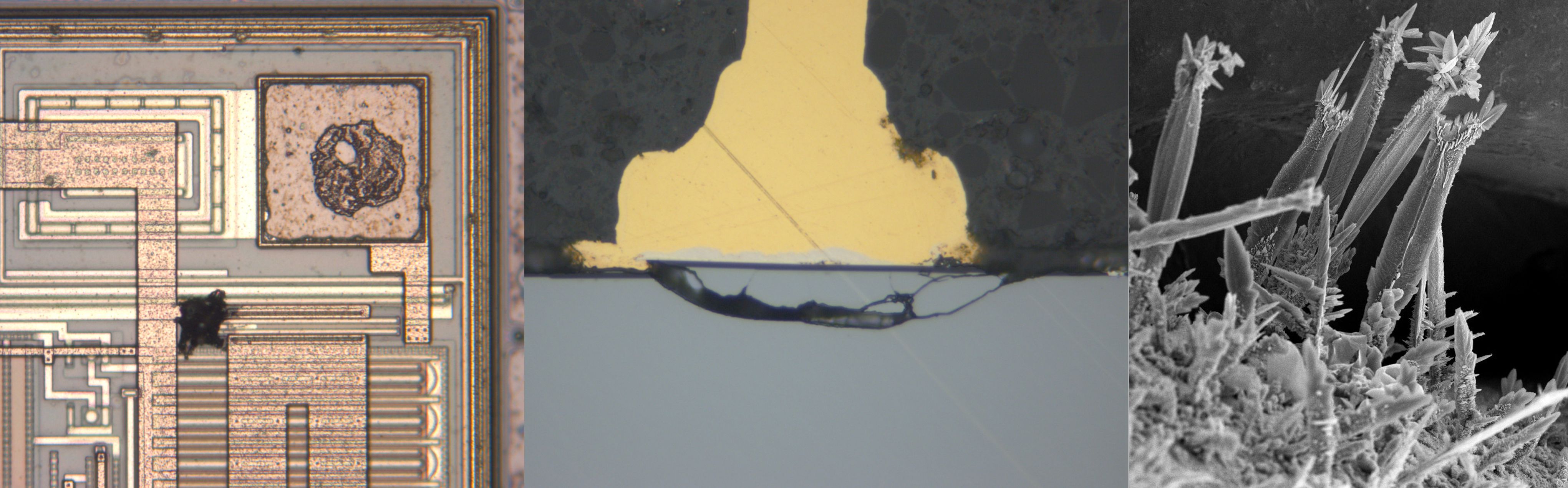
Material- and Damage Analysis
Evaluation of production materials (solder, solder paste, flux, adhesives), electronic components, printed circuit boards and assembled modules by
- wetting force measurement
- mechanical testings
- determination of layer thickness
- cross-section preparation
- scanning electron microscopy and EDX analysis
- microfocus X-Ray imaging
- computer tomography
- acoustic scanning microscopy
- infrared spectroscopy (FTIR analysis)
- etching of solder joints and copper metallization
- decapsulation of molded packages
- detection of lead
Contamination, Corrosion and Residual Substance Analysis
- identification and localization of residual substances
- surface resistance measurements
- evaluation of coatings (thickness homogeneity, curing)
Assessment of Manufacturing Quality according to Industry Standards
Solder joint assessment according to IPC-A610:
- solder meniscus formation
- solder fill in Through-Hole Technology
- de-wetting
- detection of solder joint properties like contact angle, metallurgical structure, grain boundary layers (phase formation), short circuits due to solder bridges and -beads, open contacts, missing solder, infringement of isolation clearance, incomplete liquefaction
- component positioning (lateral displacement, rotation error, polarity, overhang)
- tombstoning
- component damage by thermal overload (popcorning, pad lifting)
Electrical Measurement
- verification of specification datasheet
- high frequency parameter analysis up to 40 GHz
- measurement in climate chamber
Reliability Assessment
Degradation by thermal and/or mechanical loads:
- cracks in solder material by aging
- substrate damage
- dissolution effects on printed circuit boards and components
- documentation of solder alloy microstructures and interfaces
- identification of inter-metallic phases