
Vertical GaN Power Transistors for Compact and High-Performance Electronics on 200-mm Wafers

Higher Performance in Less Space Requires New Semiconductor Concepts

Power electronic systems are expected to deliver increasingly higher power with lower energy losses, smaller footprints, and high reliability. Conventional silicon devices are approaching technological limits, including in terms of on-resistance, switching speed, and power density. Silicon carbide offers high performance but is associated with high costs, particularly for certain low-voltage applications.

Gallium nitride (GaN) opens up new possibilities for high-performance and compact power semiconductor devices due to its material properties. However, lateral GaN devices can utilize this potential only to a limited extent as currents and voltages increase. In vertical GaN devices, by contrast, the current flows through the semiconductor volume, enabling new device concepts.

Manufacturing these devices places demanding requirements on materials and processes. These include thick, high-voltage-capable GaN layers, controlled defect and stress management, and backside processing. The handling of thin semiconductor layers, reliable electrical contacting, and assembly and interconnection technologies must also be considered.

For future industrial use, it is also essential to transfer the processes to large wafer formats and develop reproducible manufacturing processes.

From Vertical GaN Devices to System Integration

8" GaN-EPI wafers with HEMT devices

Fraunhofer ISIT develops vertical GaN power transistors for low- and high-voltage applications. One focus is on GaN trench MOSFETs with a vertical current path and on process integration on 200 mm wafers.

The work includes the development and optimization of individual process modules and complete manufacturing processes. These include trench structures, metallization, passivation, and backside contacts. ISIT also develops thin and membrane-based GaN devices and investigates their integration.

ISIT combines process and manufacturing technology with packaging, power electronics, system integration, modeling, and reliability analysis. This allows different levels of development to be addressed, from the individual device to its integration into power electronic systems.

Various collaboration models are available for joint development activities. These include research and development contracts, publicly funded collaborative projects, joint demonstrators, and development and technology transfer projects.


Jointly Assess the Feasibility of Vertical GaN Devices


Vertical GaN Trench MOSFETs Combine Material Advantages with Scalable Process Integration

Gallium nitride is a wide-bandgap semiconductor. The material offers high breakdown strength, high electron mobility, and low switching charge. This makes it suitable for devices operating at high switching frequencies and for applications with elevated operating temperatures.

In vertical GaN devices, current flows through the semiconductor volume. This concept enables high current-carrying capability and efficient use of the chip area. In trench MOSFETs, the gate structure is integrated into vertical trenches. This enables compact device structures with a vertical current path.

Process Integration on 200 mm Wafers

ISIT develops process integration based on GaN-on-QST. This material platform enables the development of thick GaN layers on 200 mm wafers, providing a basis for investigating manufacturing processes that are suitable for industrial applications.

Another research focus is the removal or thinning of the carrier substrate followed by backside contacting. Different levels of integration are being investigated:

  • Devices with a stabilization substrate
  • Thinned carrier substrates
  • Free-standing GaN membranes

The goal is to reduce additional electrical and thermal resistance within the device structure. At the same time, challenges such as mechanical stability, wafer warpage, handling, low-stress metallization, and reliable electrical contacting must be addressed.

Modeling and Characterization

Technology development is supported by simulation, material analysis, and electrical characterization. TCAD and SPICE simulations as well as electrical, thermal, and mechanical models are used.

Structural and materials analysis capabilities include scanning electron microscopy (SEM), focused ion beam (FIB), transmission electron microscopy (TEM), X-ray analysis, and atomic force microscopy (AFM).

Parameters investigated include:

  • On-resistance
  • Leakage current
  • Breakdown voltage
  • Switching behavior
  • Thermal resistance
  • Mechanical strength
  • Wafer uniformity and yield

Reliability testing includes high-temperature reverse-bias testing (HTRB), double-pulse testing, temperature cycling, and power cycling.


Discuss Process Development and Characterization for GaN Devices


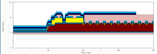
Schematic cross-section of a trench MOSFET

Vertical GaN Devices Address Power-Dense Applications from Mobility to Energy Systems

The development of vertical GaN power transistors is relevant for applications requiring high power density, efficient switching, and compact designs.

Mobility and Automotive

Potential applications range from traction inverters and electric drives to onboard electrical systems, DC/DC converters, and electric auxiliary systems. Charging infrastructure as well as electric pumps, fans, and compressors are also relevant applications.

Industry and Automation

Potential industrial applications include motor inverters, servo drives, robotics, machine tools, and industrial power supplies. High switching frequencies and compact power electronics are particularly relevant for power-dense and dynamic drive systems.

Data Centers and Information Technology

Server power supplies, point-of-load converters, DC/DC converters, and compact high-frequency converters represent additional potential applications. The focus is on power-dense power supply systems for data centers and digital infrastructure.

Energy and Power Grids

Additional applications include solar inverters, wind power systems, battery energy storage systems, bidirectional DC converters, charging systems, and energy storage technology.

Aviation and Electric Aircraft

Compact electric drives and weight-optimized power electronics for electric aircraft and unmanned aerial vehicles are also potential applications.

Vertical GaN devices may also be relevant for high-power and high-frequency converters, telecommunications and networking equipment, fuel cell systems, and electric pumps and actuators.

Vertical GaN Technology Creates Potential for More Efficient and Compact Power Electronics

Vertical GaN devices combine the material properties of gallium nitride with a vertical device architecture. This approach provides the basis for high-performance GaN devices with compact chip areas.

Development on 200 mm wafers also provides a foundation for scalable manufacturing processes suitable for industrial applications. Larger wafers and more compact chip areas offer the potential for more efficient material utilization and cost-effective manufacturing. The actual economic benefits depend on the specific process, device design, and manufacturing scenario.

ISIT's approach extends beyond the individual semiconductor device. Semiconductor and process development are combined with packaging, module and system integration, modeling, and reliability testing. This allows interactions between the device, package, and final application to be considered during development.

Research Projects

Learn more about our related research projects:

APECS

IGaNstack

VerGan