Unrivaled to small and powerful microchips
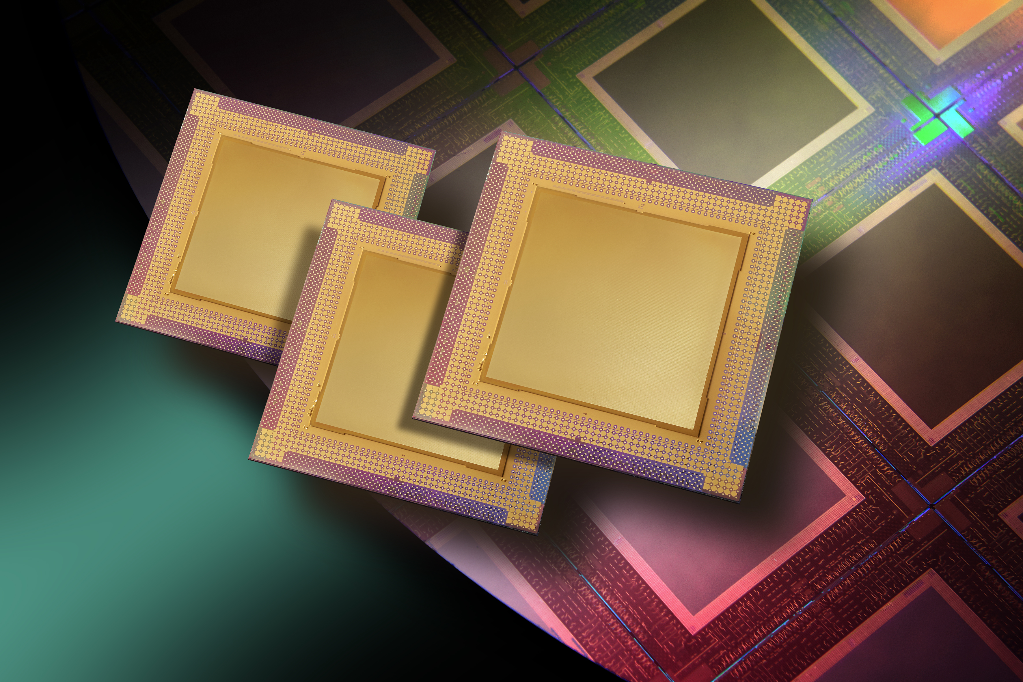
Fraunhofer ISIT and project partner IMS Nanofabrication ('IMS') have jointly developed the MEMS processing of a CMOS chip designed by IMS, which pushes the limits of what is technologically possible and represents a crucial key component for further miniaturization in semiconductor micro- and nanoelectronics.
The challenge:
For decades, the semiconductor industry has strived to optimize the power consumption, switching speed and area requirements of electronic components through miniaturization. After more than 50 years of continuous miniaturization of structures, the current major technical and physical barriers lie in the imaging technologies of photolithography, and specifically in the fabrication of high-resolution photomasks. Photomasks are needed in every chip fabrication to transfer the micro- to nanometer-sized structures that define the chip onto a photoresist-coated silicon wafer.
A technology node (smallest structure size) defines an achievable miniaturization level and thus the manufacturing processes based on it. By falling below the 10 nm technology node a few years ago, EUV lithography with a wavelength of only 13.5 nm became indispensable for further technical development.
For the fabrication of photolithographic EUV masks, techniques are needed that allow the definition of very small structures sufficiently fast and efficiently. So-called electron beam mask writers are used for this purpose.
If EUV masks with a high density of complex geometric structures are to be written, the current single-beam electron mask writers reach their limits. Limiting factors here are both the large amounts of data required to define such masks and the writing time required to produce them on the mask substrate. Single-beam electron mask recorders, for example, would require several days of writing time for a complex EUV mask.
The solution:
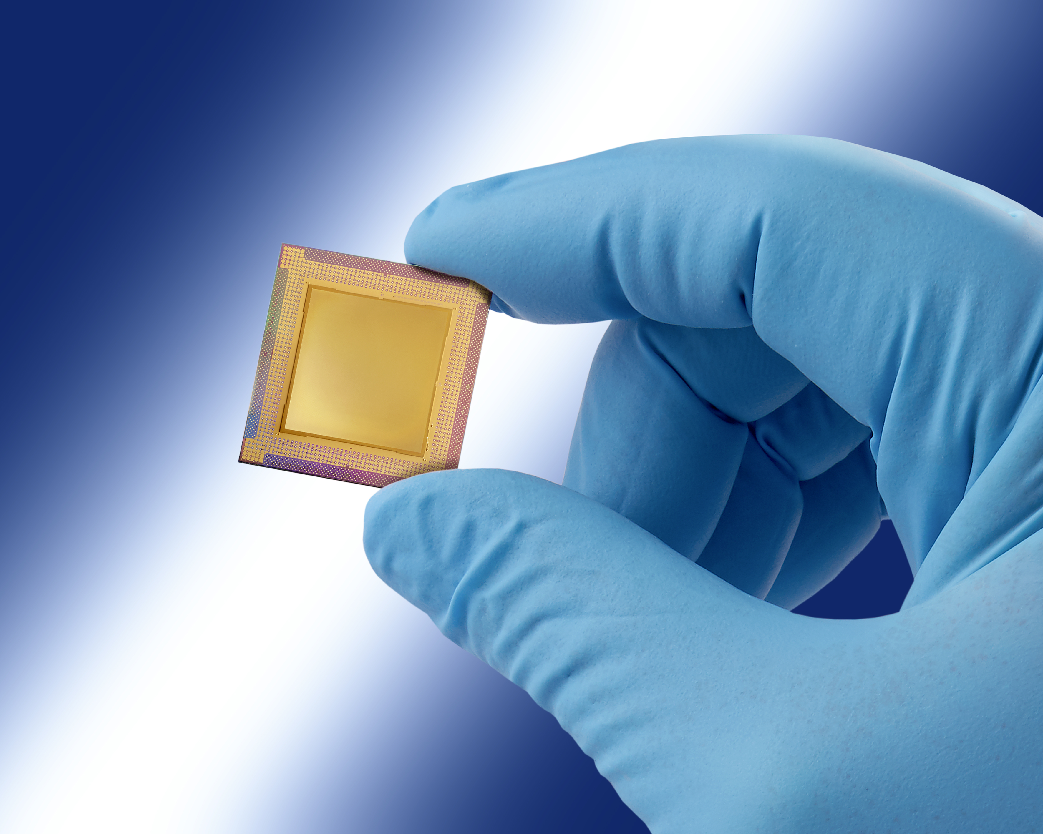
The technical and economic conditions were the motivation of the electron multi-beam mask writer (MBMW - Multi-Beam Mask Writer) developed by IMS, whose core is the TROM2 chip - an electronically controllable "pinhole" processed by MEMS technology for parallel deflection of many electron beams.
Integrated into this chip is advanced CMOS electronics with signal processing and circuit logic. On top of these electronic structures is the jointly developed MEMS design, which ensures that the electron beams fly through the chip while being individually deflected.
The TROM2 chip combines state-of-the-art CMOS high-speed signal processing with MEMS technologies. The entire MEMS process consists of over 200 individual steps and combines, among other things, high aspect ratio electroplating technologies, the Deep Reactive Ion Etch (DRIE) process based on the so-called BOSCH process, and anisotropic KOH etching of silicon.
 Fraunhofer Institute for Silicon Technology

