 Fraunhofer Institute for Silicon Technology
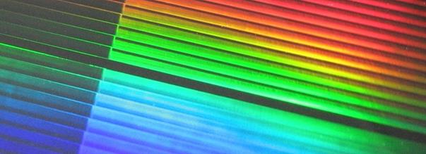
Using the Laser Annealing method at a laser wavelength of l = 515 nm, it is possible to activate both near-surface implanted dopants and to selectively modify the surface properties of materials.
At Fraunhofer ISIT, the laser process is used to anneal thinned and supported substrates (d ≥ 40 μm) with diodes or IGBT power devices. This is done within an industrially used production environment.