 Fraunhofer Institute for Silicon Technology
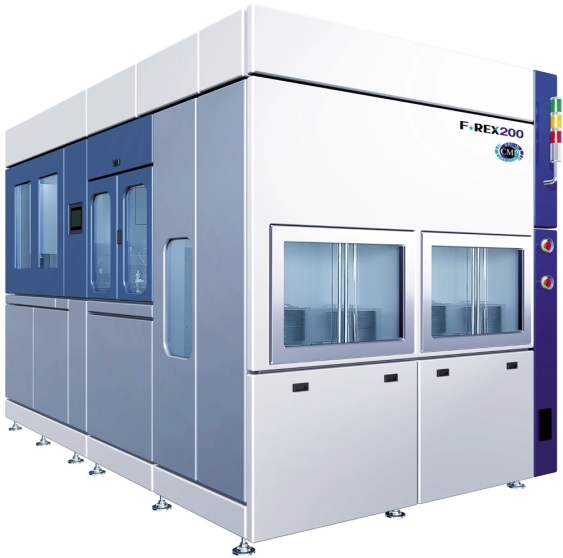
Chemical-mechanical polishing is a key technology in the production and processing of silicon wafers and other semiconductor materials. CMP is one of the technologies that make the realization of state-of-the-art microelectronic devices and micro-electro-mechanical systems (MEMS) possible in the first place.
In semiconductor technology, CMP is the method of choice when surfaces need to be planarized and smoothed with high precision. Planar and very smooth surfaces are e.g. Prerequisite for photolithography processes in the manufacture of modern integrated circuits (ICs), since the depth of field of high resolution steppers or scanners is very limited and the imaging of structures with smallest widths only on very flat surfaces are possible. Today's state-of-the-art circuits with 10 or more wiring levels and smallest line widths of 10 nm can therefore only be fabricated using CMP. The replacement of aluminum interconnects by copper metallization for very fast circuits in the GHz range is only possible through the use of so-called damascene technology, in which the repolishing of embedded metal tracks by means of CMP plays a crucial role.
Chemical-mechanical polishing is a combination of mechanical abrasion by abrasive particles and a simultaneous chemical etching attack of the surface to be polished by appropriate chemical components. Using CMP, surfaces with local roughnesses in the single-digit angstrom range and a global residual topography over the wafer in the two-digit nanometer range can be achieved.
Besides applications in the field of microelectronics, CMP has meanwhile found its way into the production of microsystems, where always flat and smooth surfaces are needed, e.g. Wafer bonding, optical components or various other new manufacturing techniques. For some time now, CMP processes have also become increasingly important in the finishing of wafer-thin processes and the production of vertical contacts through the silicon wafer (through-silicon vias (TSVs) or through-glass vias (TGVs).
The CMP facilities available at ISIT:
- Peter Wolters PM200 cluster tool (metal contaminated) for 4 ", 6" and 8 "wafers in manual handling
- EBARA FREX200 cluster tool (one track CMOS compatible and one track metal contaminated) for 8 "wafers for industrial production
- 6 "Logitech bench polisher for easy removal testing
Available measuring technology:
- Sentech-Axiotron (with Zeiss microscope) for the measurement of transparent layers (oxide, silicon, nitrides up to limited thicknesses)
- CDE Resmap 278 4-Point Prober (Four-Point Probe) for Coating Thickness Measurement of Conductive Layers
- Sartorius Analytical Balance for gravimetric measurement of layer abrasion via specific material density
- Dektak profilometer for topographic surveying of surfaces
- Optical control of surfaces by Haze lamp on unwanted particles and nanoraucies
- Zeiss microscope with dark field
- White light interferometer for measuring surface roughness (except oxide)
- Atomic force microscope for measuring nanotopographies and surface roughness
- Surfscan for automatic measurement of surface cleanliness
Wafer cleaning:
- Mega / Ultrasonic cleaning
- Semitool SAT for 4 ", 6" and 8 "wafers
- Scrubber cleaning (PVA brushes) for 6 "and 8" wafers
- Materials editable at the ISIT by CMP (no exposed gold may be traded in the CMP clean room):
- Silicon (mono, poly, epi-poly, amorphous, with impurities such as boron, phosphorus, germanium doped material)
- Oxide (thermal, TEOS, PE, LP, etc.)
- Glass (Quartz, EagleXF, Borofloat, BPSG, etc.)
- Nitride (SiN, AlN, TiN, TaN, GaN, etc)
- metal (Al, W, Cu, Ti, Ni, Mo, etc,)
- plastic (polyimide, BCB, etc.)
Application areas:
Wafer thin, surface smoothing