 Fraunhofer Institute for Silicon Technology
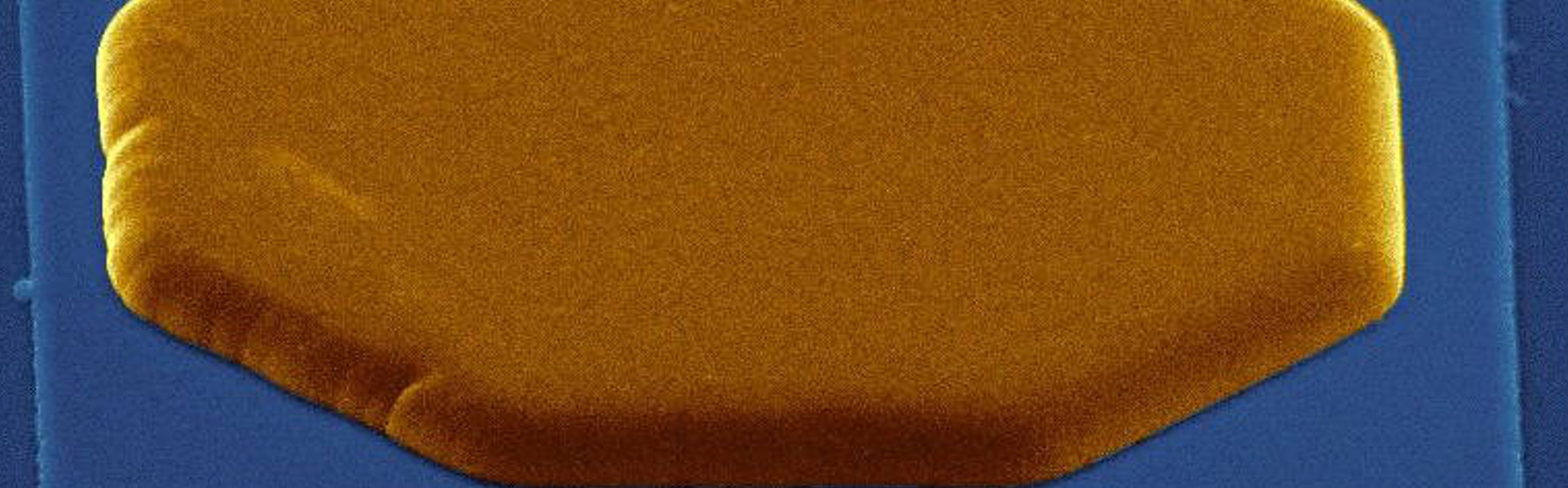
For low-cost flip chip contact bumping without wiring or for sinterable contact metallization, Fraunhofer ISIT offers a chemical, i.e. template free, deposition of Nickel (Palladium) and Gold (ENIG or ENEPIG). Deposition can be made on aluminum as well as copper pads. Since the process is performed in a batch without any lithography the deposition is considerably cheaper than a conventional galvanic process.
The infrastructure is designed for wafer diameter up to 200 mm. Due to our long-year experience with a large variety of customer wafers, this coating process runs very stable. Preferrably, the wafers will be treated with the chemical Ni-Au UBM first, followed by, further process steps like thinning, bumping or sawing. With our technological approach “UBM first” the risk for wafer breaking is strongly reduced.
Nevertheless the deposition on thinned wafers is possible as well, however, additional process steps for backside protection may be required. Very good results have been achieved on TaikoTM wafers with a backside which was passivated after grinding.