 Fraunhofer Institute for Silicon Technology
The PSM-X2 technology platform uses a low-stress, 10-30 µm thick polysilicon layer to generate static and moving sensor structures. By using high-resolution lithography, minimum structure widths down to 0.5 µm can be realized.
For capacitive detection of movements perpendicular to the plane, additional counter electrodes are implemented. This gives the possibility to excite and detect also so-called out-of-plane motions. Additive, functional layers increase the reliability and robustness of the MEMS element (e.g. anti-stiction, shock resistance).
Wafer-level encapsulation of the device elements is integrated into the process. The tight bond between sensor and lid wafer, the so-called wafer-level packaging, is created here by a gold-silicon eutectic at about 400°C. The metallic bond frame ensures a hermetic seal so that the pressure set during the bonding process is maintained over the entire service life.
By integrating a getter layer, an internal pressure of up to 10-6 bar can be achieved. The use of the novel Multi Pressure WLP Technology allows the setting of different cavity internal pressures on wafer level. The PSM-X2 platform is currently used in the field of inertial sensors, micromirrors and electron-optical deflection units.
Fraunhofer ISIT has developed an innovative manufacturing technology for the production of high-performance MEMS scanners, the so-called "two-layer epi-polysilicon process". Following the PSM-X2 fabrication technology for inertial sensors, which is already well established at ISIT, the scanners are structured from two 30 µm thick epipoly silicon layers. In this way, height-shifted finger electrodes can be realized, which can be used both for electrostatic drive of the scanners and for capacitive position detection of the mirror position.
Poly Silicon MEMS Technology Platform
Thanks to its outstanding properties, polysilicon (poly-Si) is one of the most important materials for manufacturing free-standing, moving microstructures for MEMS. However, standard semiconductor technology processes can only provide it in thicknesses of a few micrometers, which is insufficient for many applications. For this reason, the fabrication of thick poly-Si layers in an epitaxy reactor was established at Fraunhofer ISIT. In addition to the thick poly-Si, several LPCVD layers required to produce the free-standing microstructure are also part of the core of the EpiPoly technology platform.
Material |
Possible thicknesses |
Typical thickness |
Electrical resistance |
Typical function |
Epi-Poly-Silicon |
1…40 µm |
< 10 mΩ×cm | free standing micro structure | |
LPCVD-Poly-Silicon |
≤ 1 µm |
0.5 µm | < 1 mΩ×cm | Rewiring under the epi-poly |
LPCVD-Silicon oxide |
≤ 2 µm |
various insulation layers or sacrificial layer |
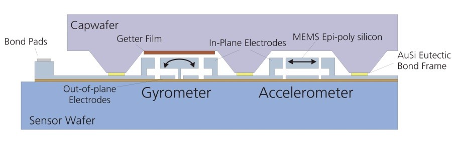
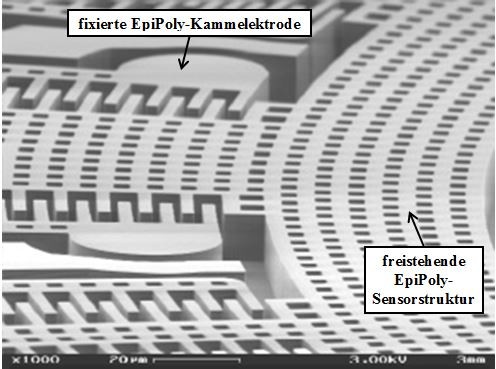
The SEM image in Fig. 1 shows the 11 µm thick, free-standing EpiPoly sensor structure of a rotation rate sensor. By means of comb electrodes made of the same EpiPoly-Si, one side of which is fixed to the substrate, the sensor structure is electrostatically excited to resonant in-plane oscillation. If an angular acceleration acts on the sensor structure, it is additionally excited to oscillate perpendicular to the plane. This oscillation can be detected capacitively by means of electrodes made of thin LPVD poly-Si located below the sensor structure, the out-of-plane electrodes in the cross-sectional image. The gap between the out-of-plane electrodes and the movable EpiPoly sensor structure is created by etching out an LPCVD silicon oxide layer in HF gas phase that was originally located in between. By bonding another Si substrate with etched cavities and getter film integrated therein, the exposed sensor structures are hermetically encapsulated, see cross-sectional image. An exclusive, patented technique of ISIT allows to set different gas pressures in adjacent cavities. This enables highly integrated, precise and cost-effective manufacturing of IMUs (Inertial Measurement Units) with acceleration and angular rate sensors on one and the same chip.
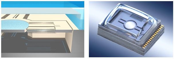
Fig. 2 on the left shows the schematic cross-section through an electrostatically actuated, two-axis MEMS scanner, for whose drive and sensing electrodes, respectively, two 40 µm thick EpiPoly layers were used. These also form the mirror plate, which is extraordinarily rigid thanks to a total thickness of 80 µm and does not deform during operation even with diameters in the mm range. Unlike the inertial sensors, the moving structure is exposed by removing the substrate underneath from its rear side. A sacrificial layer is not required. MEMS scanners can also be hermetically encapsulated if required. The photo in Fig. 2, right, shows a single-axis MEMS scanner with a three-dimensionally shaped glass lid and a bottom made of silicon. A getter material on the Si bottom also provides a stable vacuum inside the sealed cavity. Thanks to the vacuum, the scanner can be excited to resonate with very low voltages. The bonding of the MEMS, lid, and bottom substrates is accomplished in a single bonding process. A description of the different bonding processes for MEMS device encapsulation as well as the 3D glass technology, another exclusive technique of ISIT, can be found in the section "MEMS Fabrication Processes".
By combining the EpiPoly technology platform with other technology platforms, its application possibilities can be expanded extraordinarily. Using the piezo MEMS technology platform, for example, piezoelectrically actuated scanners can also be manufactured. Scanners with PZT-based actuation can be easily excited to oscillate even in air thanks to the very large forces. AlN- and AlScN-based scanners can be operated quasistatically. Using the PowderMEMS technology platform, NdFeB micromagnets can be integrated at the substrate level in the moving structure of a scanner. Scanners of this type can be excited by the electromagnetic fields of external coils. Again, large forces and operation in quasi-static mode are possible. In addition, the actual MEMS device does not require any electrical connections at all, which greatly simplifies its manufacture.