 Fraunhofer Institute for Silicon Technology
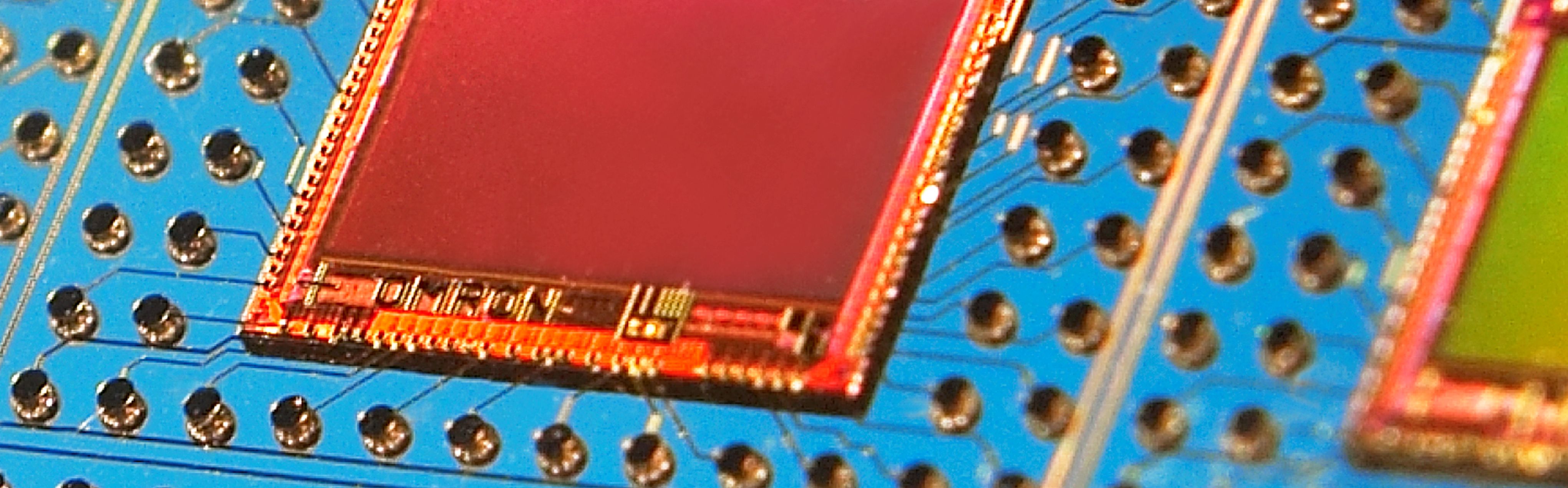
The massive increase of microstructured components in mobile electronic devices necessitates extremely miniaturised components with thicknesses below 1 mm. The Fraunhofer ISIT is specialized on the advanced hybrid integration of micro components like inertial sensors with their electronic driver circuits. This assembly concept can, depending on chip geometry and complexity, also be executed on wafer level (WL-CSP), which allows particularly thin assemblies.
The institute has developed a modular toolbox of key technologies that allow a rapid customer specific component development, like the following:
- symmetrical wafer thinning of MEMS components
- special dicing techniques, e.g. to expose wirebond pads
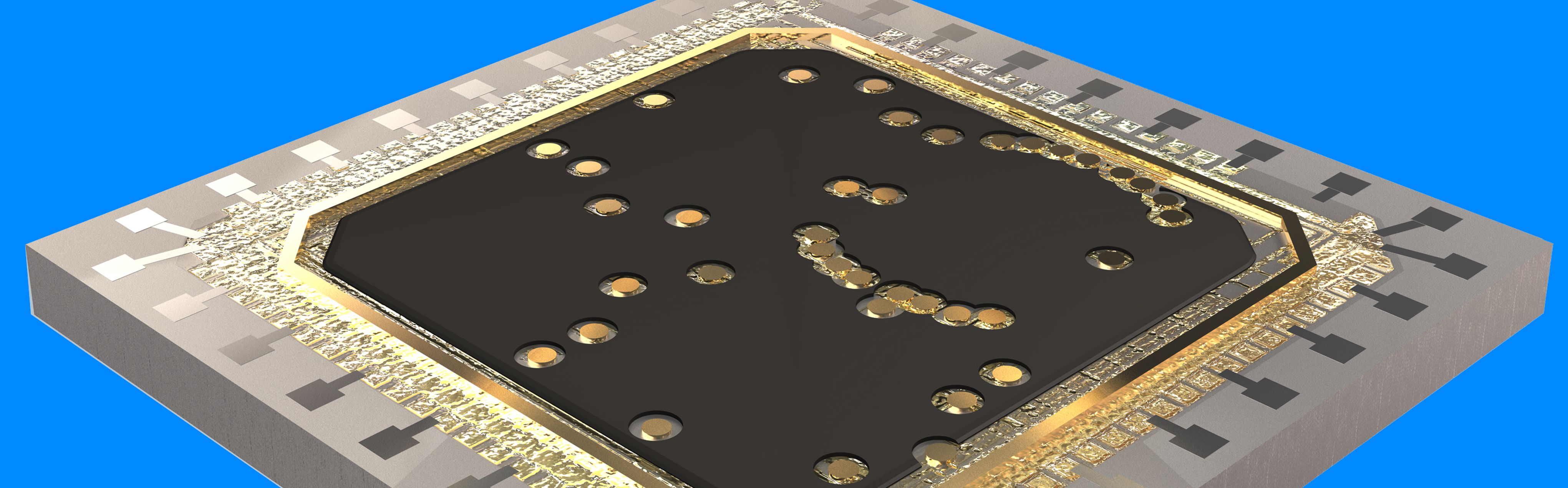
- electrical feedthrough in glass and silicon wafers (TSV: Through-Silicon Via)
- chip-stacking technique with adhesive transfer foils
- spacer technology for chip mounting
- 3D wire bonding and
- bumping and balling with solder preforms, paste or gold stud-bumps