 Fraunhofer Institute for Silicon Technology
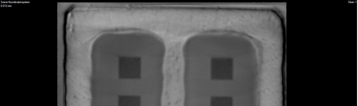
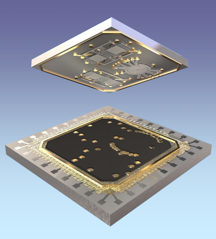
The packaging of micro components on wafer level uses the precision of semiconductor and microsystem technologies to realize robust and extremely compact setups. The special focus at ISIT is on the hermetic (vacuum) capping of microsensors and actuators as well as microoptical components using different joining technologies such as glass solders or metals (IR imager wafers with IR windows made of Si). For micro-optical components, packages with optically transparent window areas for the visible range to far infrared can be produced. Wafer-level packaging is also suitable for post-CMOS processing of customer-supplied wafers. Applications for the technology platform include IR sensors and IR imagers, inertial sensors, magnetic field sensors, harvesters and MOEMS devices.
To maintain vacuum in a very small package, the outgassing and desorption of gas molecules from the enclosed surfaces must be controlled. So-called getter layers make it possible to permanently bind free molecules of most critical gas species - effectively acting as an "in-situ" pump that remains active throughout the service life of the final product.
Checking the internal pressure in a wafer-level package can be an important requirement to estimate the expected product lifetime. To date, no general-purpose method exists that is cost-effective and sufficiently accurate to apply to any MEMS. However, ISIT has developed the "Neon Ultra- Fine Leakage Test" for MEMS resonators, which allows detection of ultra-fine leaks based on the Q-factor of the electromechanical resonant circuit (damping fraction of the trapped gases) and from this a prediction of the expected pressure rise over the product lifetime.