 Fraunhofer Institute for Silicon Technology
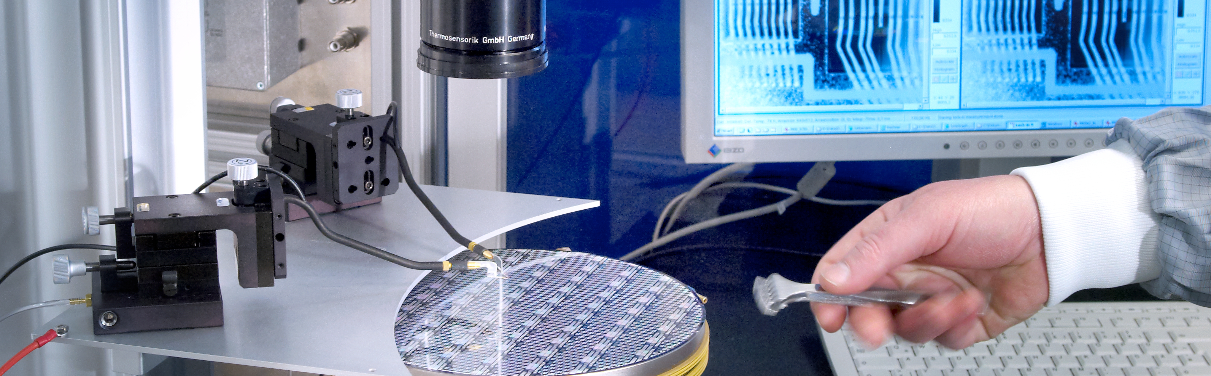
© Fraunhofer ISIT / photocompany, Itzehoe
Electrical Characterization
Tabbed contents
Our solution
Fraunhofer ISIT provides you with a professional measurement technology platform that covers all common methods of electrical characterization and also integrates state-of-the-art analysis methods:
- Static and dynamic parameter measurements (IV/CV, pulse measurements, Rds(on), switching characteristics)
- Fault analysis with lock-in IR microthermography for hot spot detection
- Structural analysis using scanning electron microscopy (SEM) and focused ion beam (FIB)
- Tests at wafer, PCB, and module level – all available 24/7 at the ISIT site
Technology
- Wafer-level tests: IV/CV characteristics, pulse and temperature-dependent measurements
- PCB & modules: Functional tests under real operating conditions, voltage resistance, switching cycles
- Lock-in IR microthermography: Localization of thermal anomalies
- SEM & FIB: Surface analyses, precise cross sections and material characterization
- Virtual cleanroom tour: Online insight into our MEMS production
Applications
- Characterization of PowerMOSFETs and IGBTs directly at wafer level
- Fault analysis for module failures in power electronics
- Parameter tests for analog and mixed-signal ICs
- Qualification of MEMS sensors prior to system integration
Benefits
- Comprehensive service: development, testing, and analysis from a single source
- Highest measurement accuracy and resolution thanks to state-of-the-art measurement technology
- Fast troubleshooting and targeted process optimization
- Permanent availability and virtual cleanroom tours
- Seamless integration of characterization and production at the ISIT site