 Fraunhofer Institute for Silicon Technology
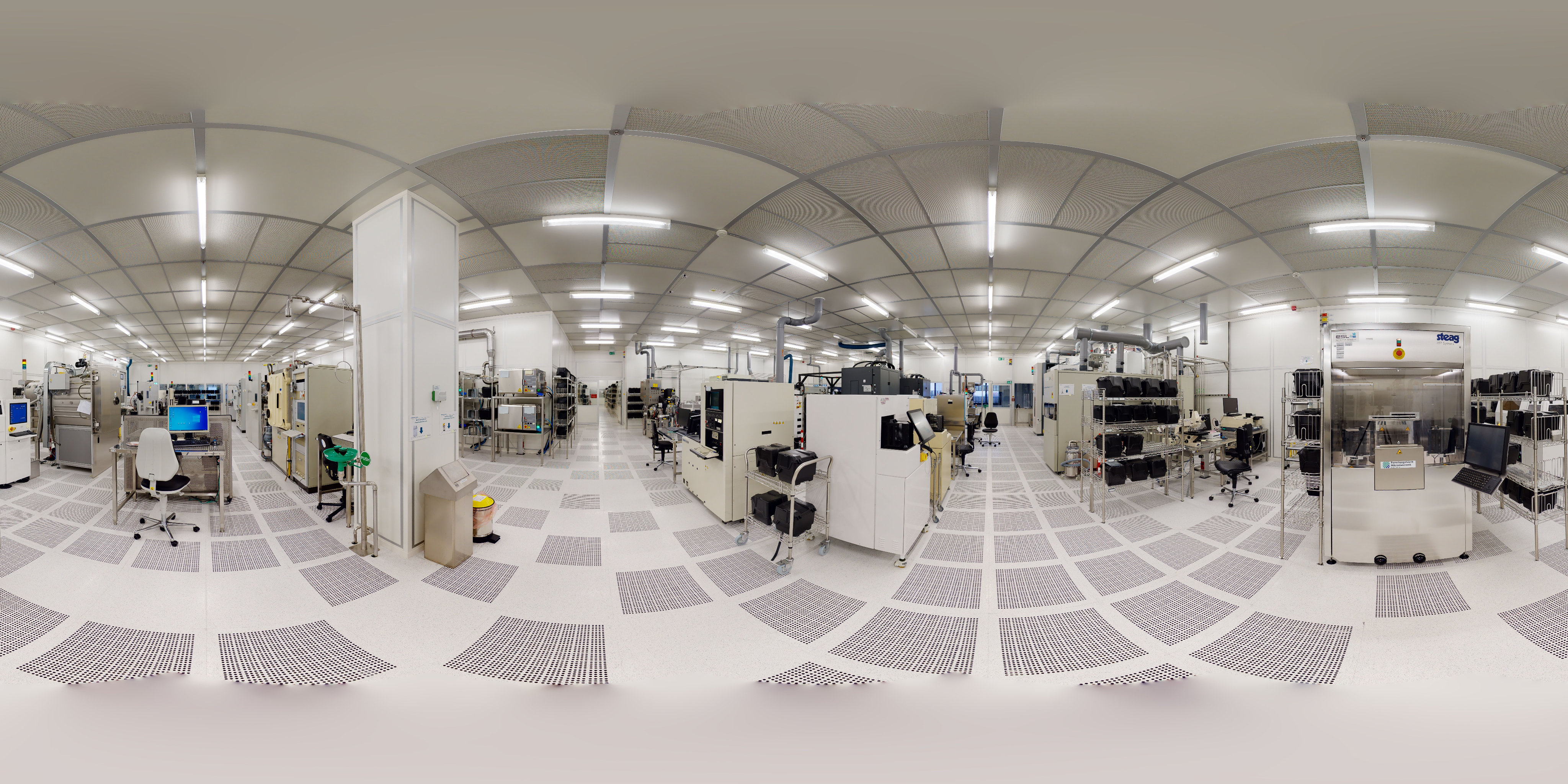
Individual processes
In addition to a complete process chain, ISIT also offers its customers the option of using only individual processes.
more info© Fraunhofer ISIT / Omnia360

Wafer-Level Packaging
Manufacturing of silicon or glass cap wafers, a variety of wafer bonding processes, and the patented “Neon ultra-fine leak test” form the basis of wafer-level packaging.
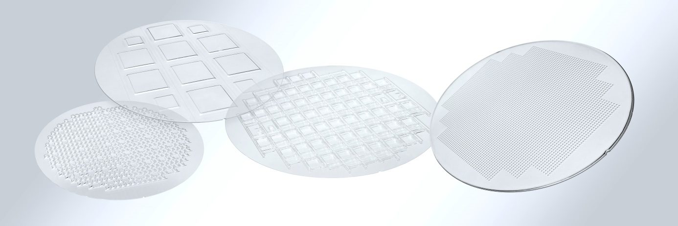
more info© Fraunhofer ISIT / photocompany, Itzehoe
Glass Micromachining
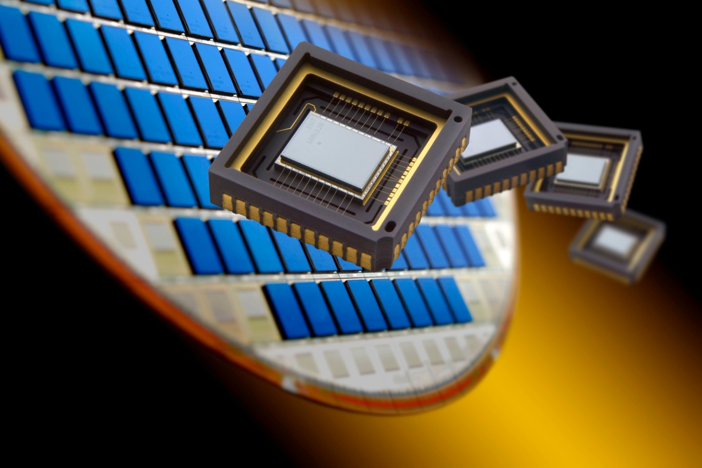
The high-temperature viscous glass flow process enables manufacturing of glass packages with spherical or inclined optical windows as well as mirrors and lenses.
more info© Fraunhofer ISIT / photocompany, Itzehoe
Wafer-Level Packaging and Processes
Fraunhofer ISIT has a modern 200 mm clean room line for the development and fabrication of silicon and glass microsystems. Due to many years of experience in the development and production of MEMS and MOEMS components, ISIT has a broad portfolio of mature individual processes as well as various process platforms. By adapting the existing processes to the respective customer requirements, individual solutions can be realized at short notice and transferred to pilot production.
One of the major challenges in the manufacture of micromechanical and microoptical systems at wafer level is the hermetic encapsulation of the components. In the context of general miniaturization, traditional metal or ceramic packages are increasingly being replaced by caps made of silicon and glass, which are already hermetically bonded to the component at wafer level. As one of the leading development service providers in the field of wafer-level packaging, ISIT has a large toolbox of processes for the realization of diverse cap wafers made of glass and silicon and their connection to the substrate.
One of ISIT's specialties is the production of lenses and glass caps using a patented glass flow process. Depending on the application, spherical or planar surfaces with high optical quality can be produced, whereby the inclination of the planar surfaces can be freely adjusted.