 Fraunhofer Institute for Silicon Technology
Sputtering and evaporation are two processes for making conductive, semiconductive, and insulating layers that have a non-crystalline structure. Thus, layers can be produced in a deposition process with amorphous and polycrystalline structure.
Sputtern & Evaporieren
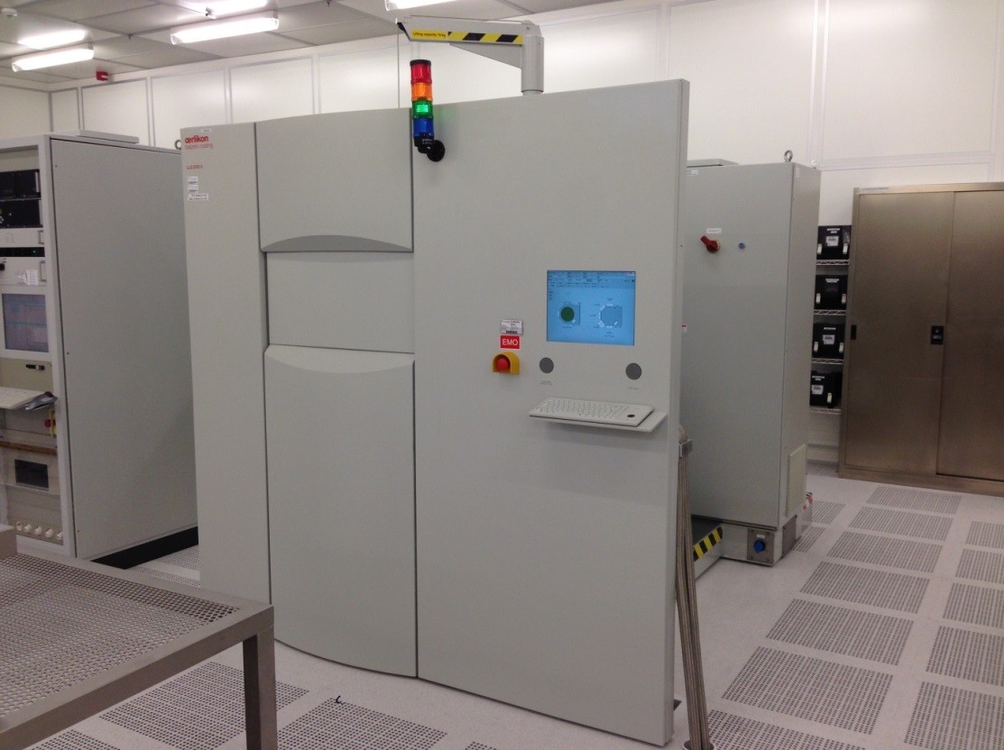
System for Sputtering
Our LLS EVO2 magnetron sputtering system from Oerlikon (Evatec) has a process chamber with 5 DC sputtering sources (one of which is RF) and a lock chamber equipped with a degas device and an RF etching device. For the high vacuum one uses the cryotechnology. The substrate basket with the substrates rotates about its own axis during the process.
Processes:
- Equipment capacity: Batch process with 8 substrates with 8 "or optionally also 16 substrates with 6"
- Metals: Ti, Cu, Cr, WTi, Au and TiN
- At the LLS EVO2 layer thicknesses
- Sputtered 20 nm to 1 micron
Application areas:
- Adhesion (adhesion) layers such as titanium or chromium
- Diffusion barriers such as tungsten titanium or titanium nitride
- Starter layers for electroplating such as gold or copper
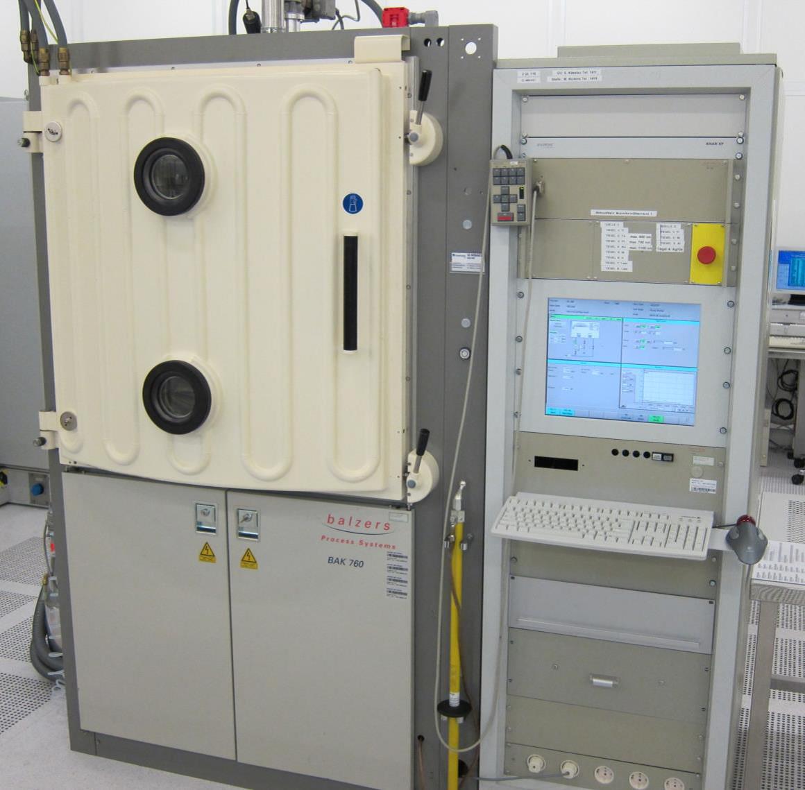
Evaporation
The ISIT has a BAK 760 vapor deposition system from Oerlikon (Evatec). The system uses electron beam to vaporize the material. It is equipped with two beam sources.
Processes:
- Plant capacity: Batch process with a maximum of 8 substrates with 8 "or optionally also 16 substrates with 6"
At present, the following metals are available for metallization: Ti, Ta, Al, Ni, Ag, Pt, Au, Ir and Ge - Layer thicknesses from 20 nm up to 1 μm
Application areas:
- Adhesion (adhesion) layers such as titanium or aluminum for the application of conductor layers
- Metallic layers such as platinum or iridium for lift-off applications
- Starter layer for electroplating
- Reflective layers for the construction of planar and convex mirror applications