Sensor technology

Magnetic bias
Integrated micromagnets for sensor technology
Our solution:
- Micromagnets integrated on substrate level
- Support fields for various magnetic field sensors (back bias, TMR, etc.)
- Various materials: NdFeB, SmCo, ferrite, etc.
Support magnets for magnetic field sensors have so far been mounted inside or outside the package. PowderMEMS enables precise integration of the magnets at wafer level close to the sensor. This enables a high degree of miniaturization, optimal magnetic field geometries and a significant saving of raw materials.
Application:
- Back bias for gear wheel rotation rate measurement
- Support field for current sensors
Flow sensors
Stabilization of thermal flow sensors
Our solution:
- Porous support structures integrated at the substrate level
- Stabilization of thin film membranes
- Modification of existing designs possible
Thermal flow sensors are conventionally manufactured on fragile thin film membranes. The failure of these membranes due to e.g. pressure surges is a common failure mode, which leads to total system failure. Our approach aims at stabilizing the membrane to avoid this failure mode.
Application:
- Thermal flow sensors in harsh environments.
- Other thin film membrane thermal MEMS such as infrared (IR) sensors.
Porous membrane - capping
Porous wafer protection caps for gas and pressure sensors
Our solution:
- Production of protective caps of various geometries in 200 mm / 8" substrates
- Wafer process: integration with MEMS wafers possible by substrate bonding
- Functionalization of the filter structure by e.g. hydrophobization, catalytic surface etc.
- Integration of heaters for use as pre-concentrator
MEMS gas and pressure sensors must be protected against harmful environmental influences such as particles or condensing moisture. Traditionally, the integration of protective caps is done as a single chip process. PowderMEMS offers the ability to produce a variety of porous protective caps in 200 mm / 8" substrates. The cap wafers can be directly bonded to the MEMS wafer – eliminating the need for single chip processes. By fabricating the protective caps in a MEMS process, further functionalization such as hydrophobation or catalytic surfaces can be achieved.
Application:
- MEMS gas sensors e.g. VOC, CO2, H2, etc.
- MEMS pressure sensors
Bio / gas sensing
PowderMEMS for gas and biosensors
Our solution:
- Fabrication of very large reaction surfaces in 200 mm / 8" Si wafers.
- Catalytic ALD surfaces and/or immobilization of enzymes
- Co-integration of heaters and electrodes
- Low footprint due to use of the third dimension
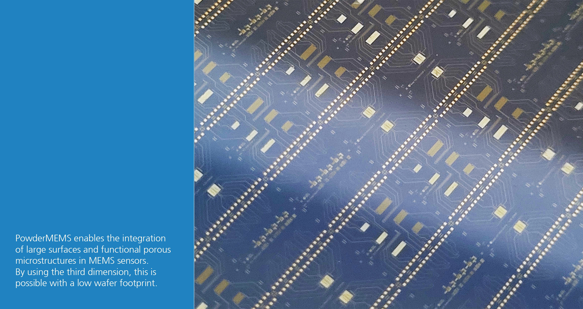
MEMS bio- and gas sensors require large reaction surfaces to achieve high sensitivity. Using PowderMEMS, porous microstructures with very large internal surfaces can be fabricated by exploiting the third dimension with the smallest footprint on 200 mm / 8" Si wafers. The inner surfaces can be modified e.g. with catalytic ALD layers or used for the immobilization of enzymes. By using established MEMS technologies, additional functional elements such as heaters and/or electrodes can be integrated.
Application:
- MEMS gas sensors e.g. VOC, CO2, H2, etc.
- MEMS biosensors
 Fraunhofer Institute for Silicon Technology