 Fraunhofer Institute for Silicon Technology
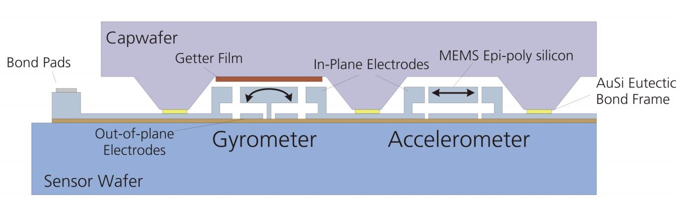
Inertial Sensors
Micro Electro Mechanical Systems (MEMS) combine small device size with low cost in production and high reliability.
more infoPoly Silicon Process Platform
An encapsulation of the components at wafer level is integrated in the process. The firm bond between sensor and lid wafer, the so-called wafer-level packaging, is created here by a gold-silicon eutectic at around 400°C. The metallic bond frame ensures a hermetic seal so that the pressure set during the bonding process is maintained over the entire service life. The metallic bond frame ensures a hermetic seal so that the pressure set during the bonding process is maintained over the entire service life. By integrating a getter layer, an internal pressure of up to 10-6 bar can be achieved. The use of the novel Multi Pressure WLP Technology patented by ISIT allows the setting of different cavity internal pressures on wafer level (large picture). The PSM-X2 platform is currently used in the field of inertial sensors, micromirrors and electron-optical deflection units.