 Fraunhofer Institute for Silicon Technology
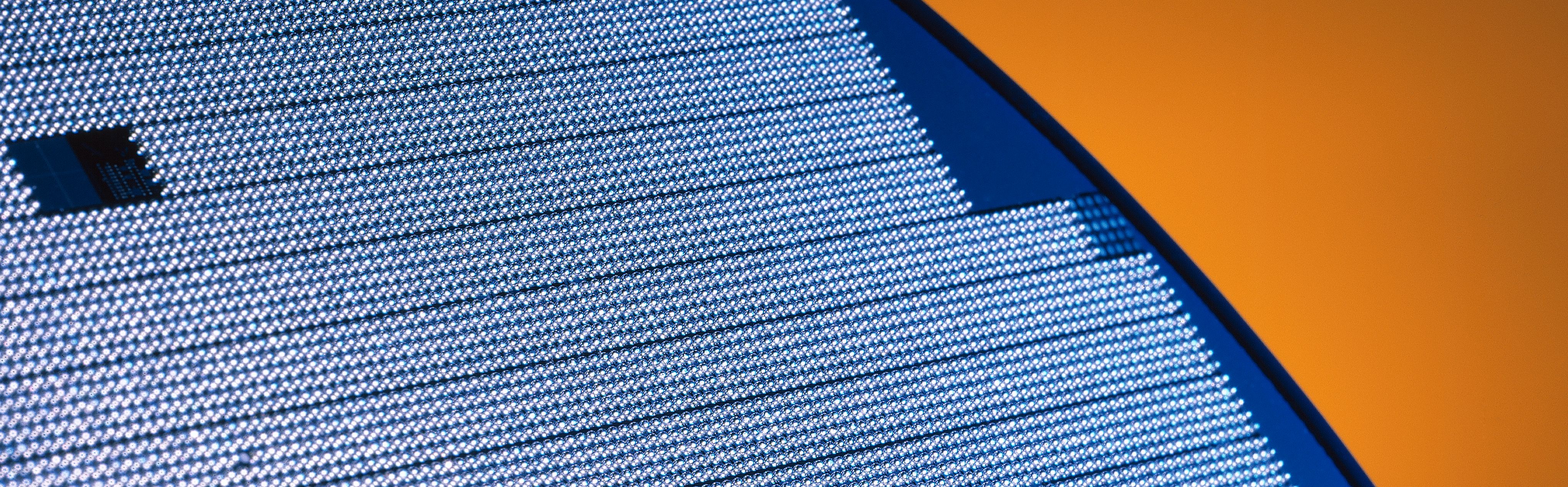
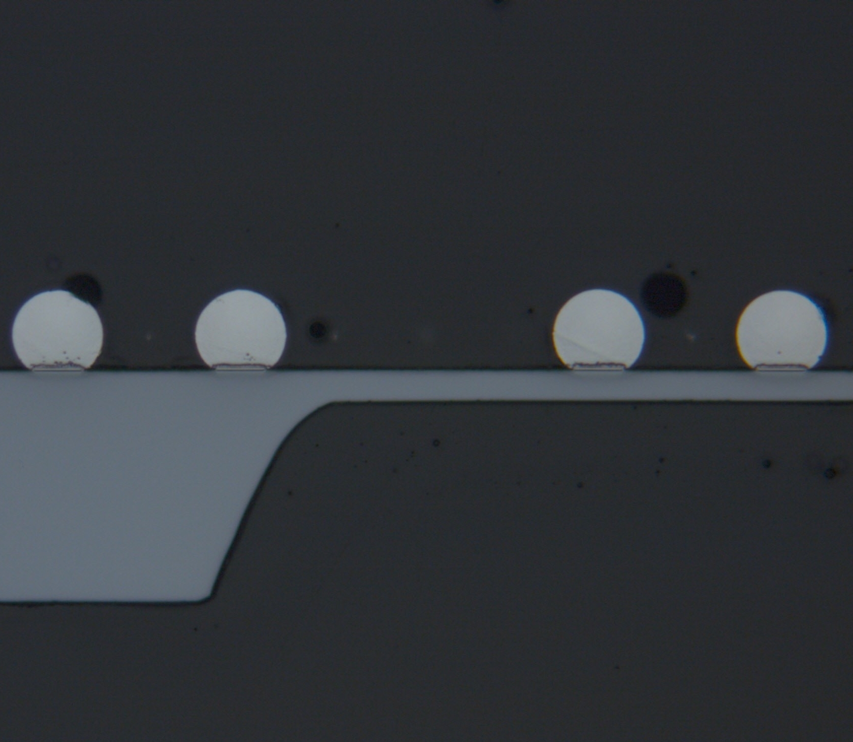
For the application of solder balls on wafer- and substrate level, ISIT can offer two technologies. WL-CSP components are typically processed on wafer level using solder ball preforms. The available infrastructure is able to provide wafers up to 200 mm diameter (300 mm wafer on request) with a NiAu contact metallization, on which the pre-formed solder balls (≥ 200 µm) are soldered in a pitch of 400 µm with a very high yield. This process is applicable for strongly thinned TAIKO wafers down to 30 µm rest thickness. Alternatively, a precision stencil printing technique is available to form flip chip solder bumps with down to 250 µm pitch in industrial quality. For demonstration, pitch dimensions down to 170 µm have already been realized.