 Fraunhofer Institute for Silicon Technology
Piezo-electrical thin films
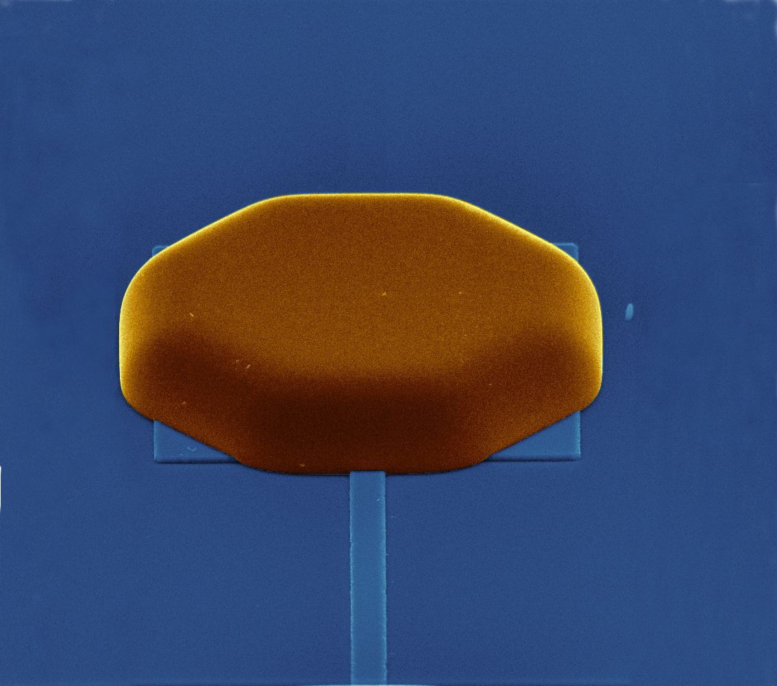
Semiconductor manufacturers usually rely on Aluminum and in some rare cases Copper as contact metallization. Unfortunately, Aluminum cannot be soldered and the copper is usually not thick enough for a reliable solder connect. A very efficient way to gain a solderable metallization is the electroless deposition of a Nickel diffusion barrier. In contrast to classical cleanroom processes the chemical deposition doesn’t require any lithography, since the Nickel is deposited only within the pad openings. The processing is carried out as a batch process, enabling a cheap process flow for high wafer counts.
To avoid oxidation of the Nickel surface a thin Gold layer is applied to cover the entire surface. In addition Fraunhofer ISIT is able to apply an intermediate layer of Palladium, which is useful to widen the process window for wire bonding applications.
Deposition is possible on 6’’ and 8’’ wafers, and with some restrictions on singulated chips from multi-project CMOS wafers. To avoid unwanted deposition on the wafer backside a passivation is required. In case of thinned wafers a foil can be applied to realize this protection. Unfortunately, this is only feasible for low wafer counts. Therefore ISIT prefers to carry out the NiAu deposition before grinding and dicing.
Processing of wafers with TaikoTM geometry has been proven to be very reliable provided that the wafer backside is passivated.
Characteristics:
Selective deposition on Aluminum and with different pretreatment Copper. Other metals and oxide free silicon have to be passivated. Nickel thickness typically between 1µm and 5µm; up to 20µm for special applications. Gold layer as oxidation protection with a typical thickness between 20nm and 70nm.
Process Steps:
- Step 1: Pad cleaning
- Step 2: Seeding with Zink or Palladium
- Step 3: Autocatalytic deposition of Nickel
- Step 4: Immersion Gold (exchange reaction)
Applications:
solderable and sinterable metallization for
- sensors
- ASICs
- power devices
- …
Equipment 1:
- in-house development
- deposition on Aluminum (AlCu) and Copper
- electroless Nickel / immersion Gold
- 6” and 8” wafers
- backside protection with tape
- handling of very thin wafers
Equipment 2:
- PacLine 300 M25
- deposition on Aluminum (AlCu)
- electroless Nickel / electroless Palladium / immersion Gold
- 8” wafers
- backside protection with tape