 Fraunhofer Institute for Silicon Technology
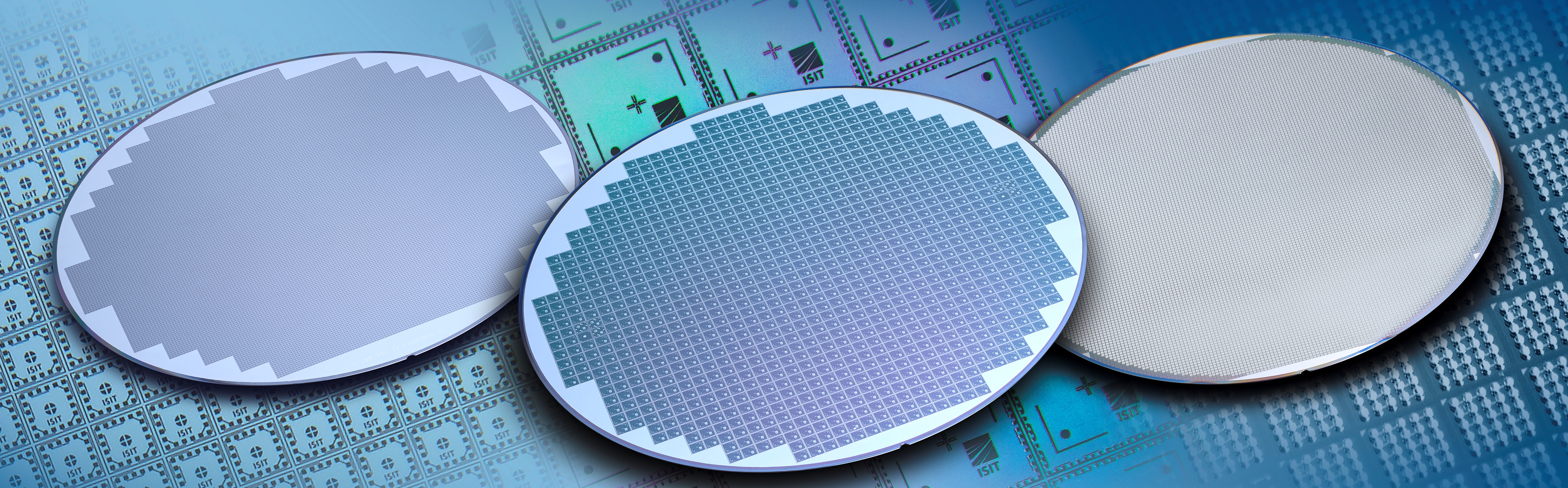
Test wafers are typically used for material screening, process development, and machine demonstration. In contrast to product wafers, which are expensive and difficult to access, test wafers can be fabricated at lower cost with additional features beneficial for the respective application. Fraunhofer ISIT offers customized wafer designs as well as standard designs for typical applications.
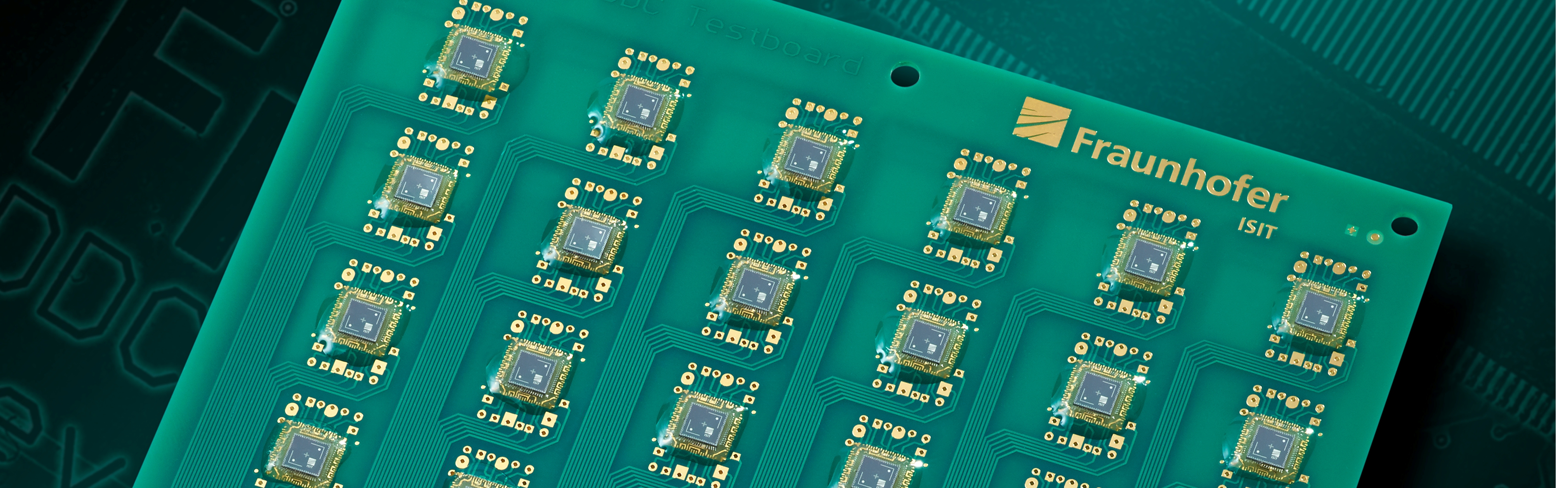
For material screening applications often silicon chips with contacts linked in pairs are used. Placed on a corresponding substrate a daisy chain is formed, which enables easy contact and short measurements. Automated measurement can be performed with a measurement electronic developed by Fraunhofer ISIT. Besides daisy chain resistance measurement and short detection, the electronics is able to determine the contact resistance of the interconnect by Kelvin probe measurements.
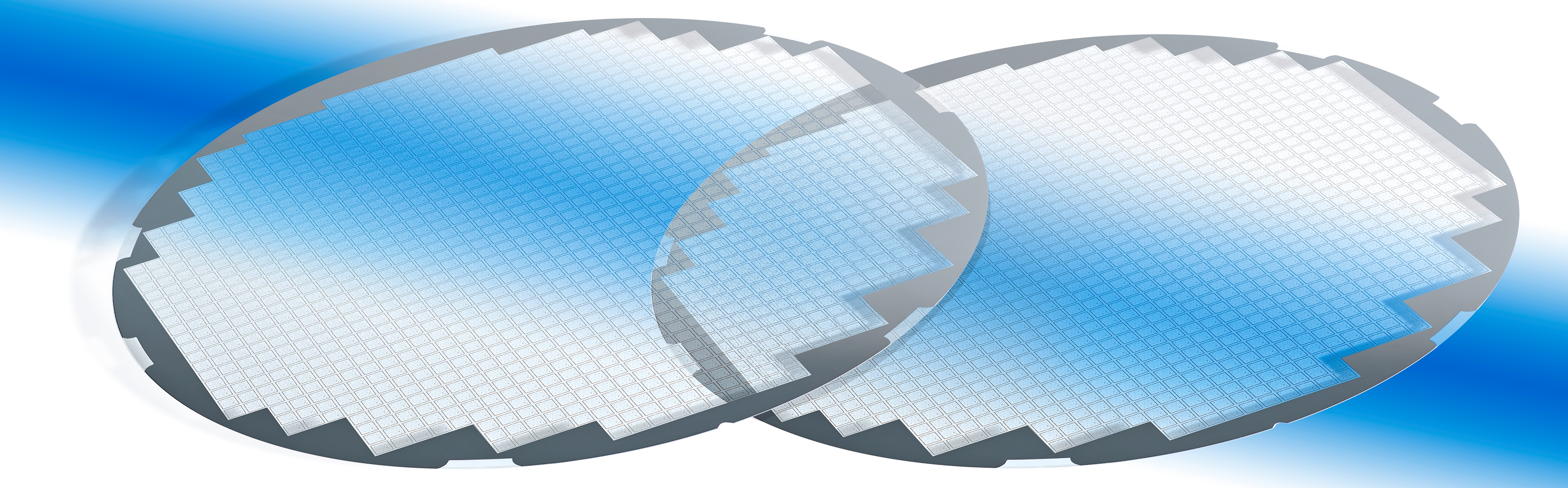
The placement accuracy of wafer aligners and die placers can be measured easily with the aid of glass wafers with precise alignment marks and Vernier structures. Automated placement of these chips is often used by equipment manufactures to demonstrate machine capability during fairs and custom handover.
Wafers manufactured by Fraunhofer ISIT are 200mm in diameter. They are produced on industrial production equipment in our in-house clean rooms. Usually, they are delivered as undiced wafers or diced on tape. Fraunhofer ISIT does not sell single chips.