Silicon Wafers

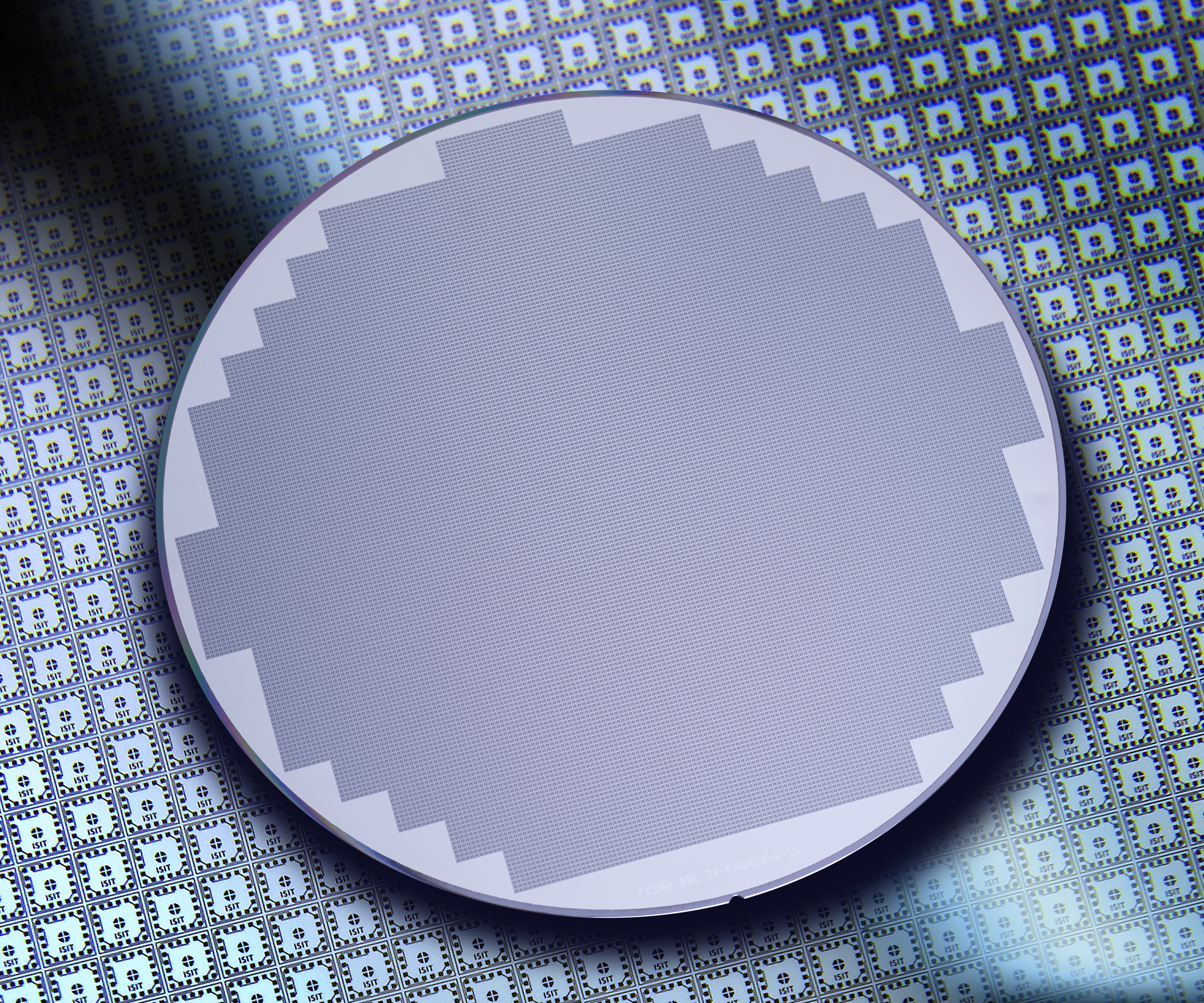
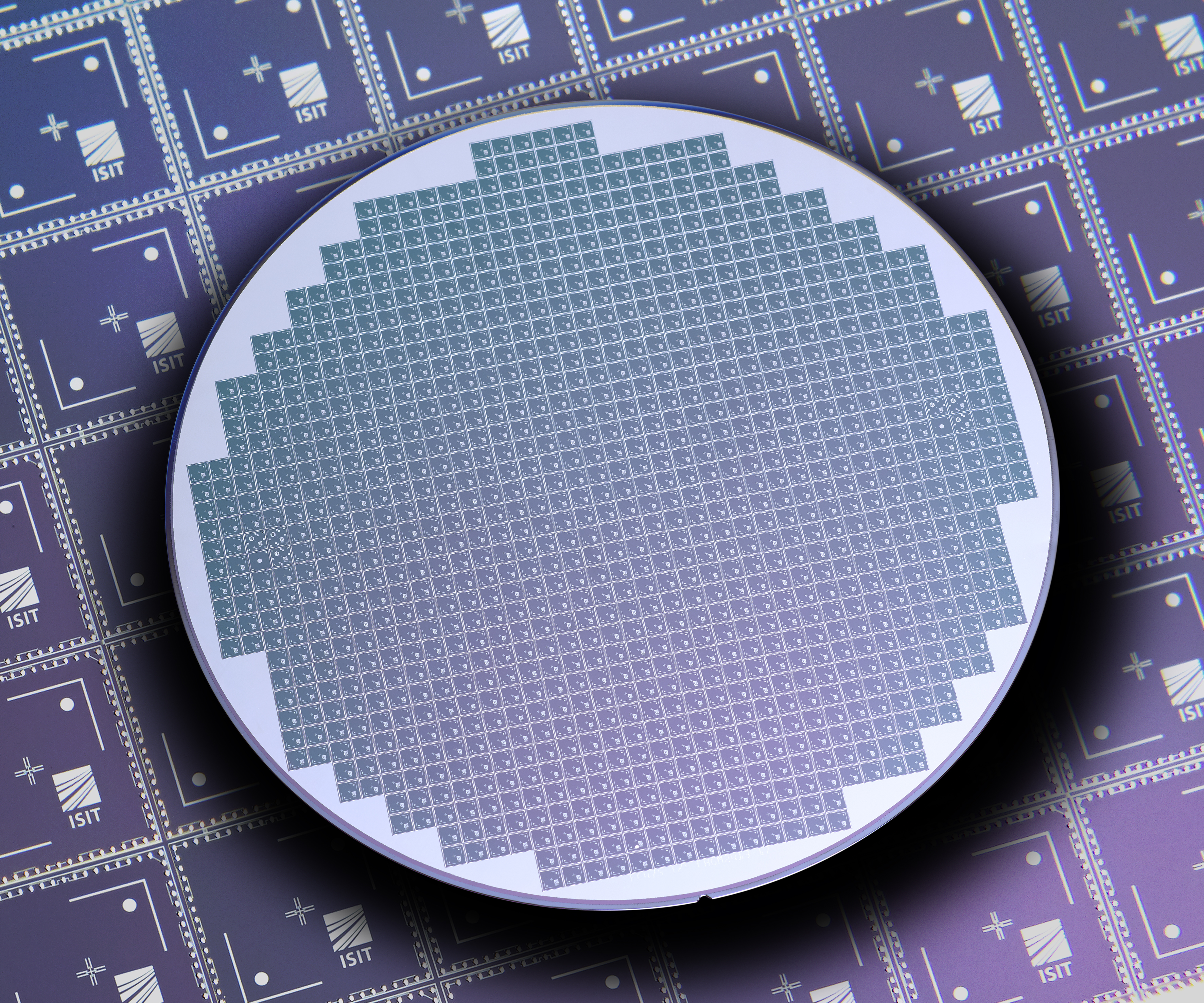
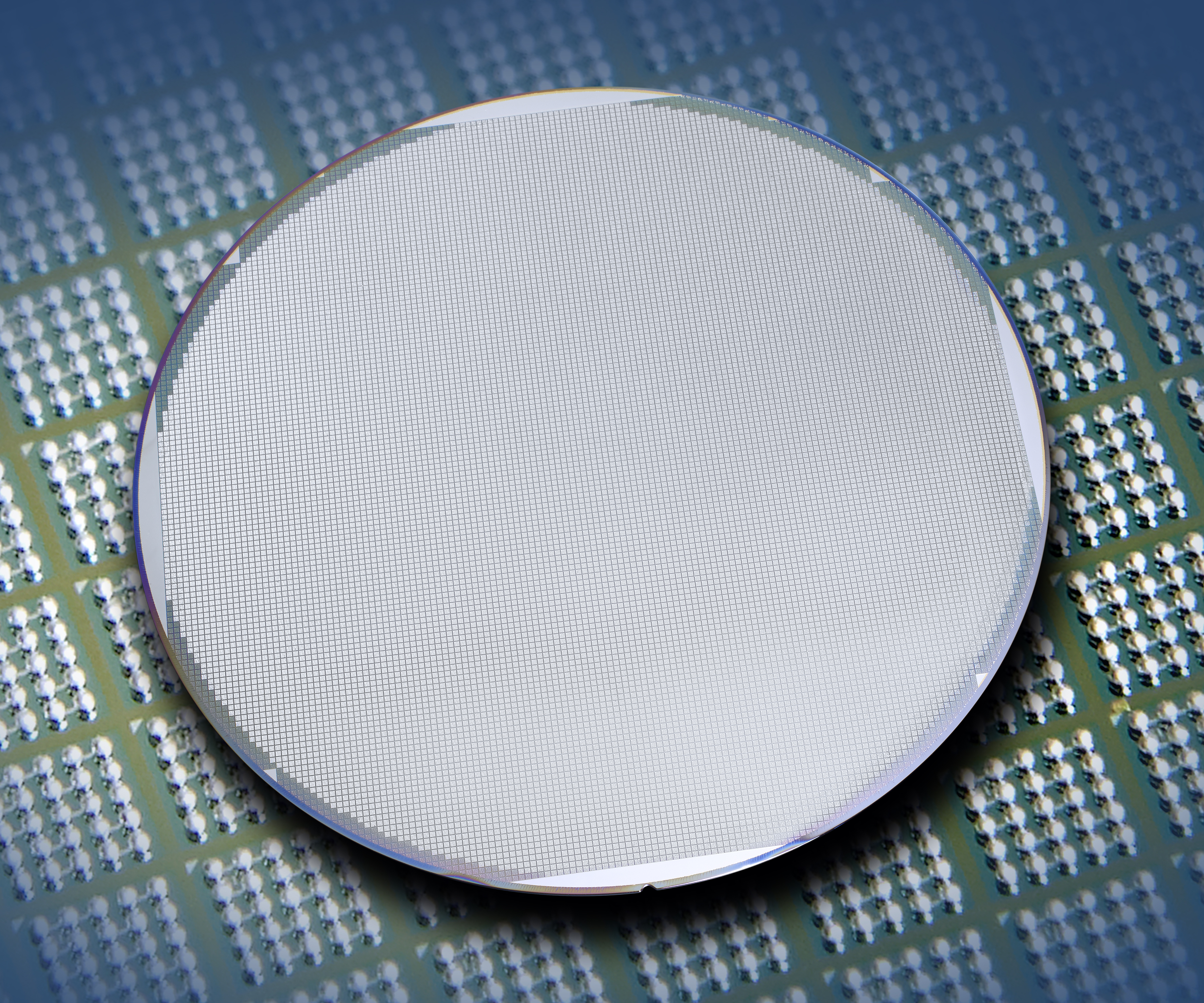
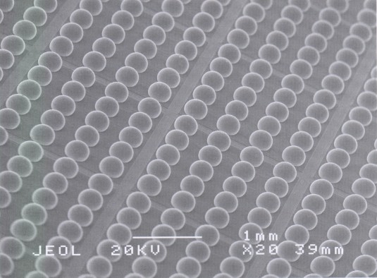
Silicon test wafers are manufactured on the same equipment as CMOS or MEMS products. Their properties with respect to mechanical behavior, surface, and contact metallization are very similar to functional commercial products. However, their fabrication is much cheaper since many production steps can be omitted. Furthermore, the design can be adapted to ease the desired tests.

Existing layouts for material screening exhibit electrical contacts connected in pairs. Combined with a corresponding substrate a daisy-chain is formed. A simple two point measurement can be used to check if all contacts are connected. Some designs feature two nested daisy chains. In this configuration a voltage between neighboring contacts can be applied to trigger whisker growth and detect shorts. In addition most designs exhibit structures for Kelvin probe measurements of the contact resistance.

© Fraunhofer ISIT / photocompany, Itzehoe

For automated measurements Fraunhofer ISIT developed a dedicated multiplexing electronic, which enables fast monitoring of defective connections in a standalone configures as well as computer aided measurement of the chips.

Customized wafers with bond frames fabricated by etching or galvanic deposition are well suited for process developments in wafer level packaging applications. Based on ISITs MEMS technology many materials can be used, e.g. aluminum, germanium, gold, copper, or tin. Even chemical nickel gold (ENIG) can be deposited selectively on wafers with aluminum pads.

Thinned, unstructured silicon wafers with surfaces prepared for gluing, soldering or sintering are often used for process and material development. With the aid of temporary wafer bonding or Taiko™ grinding wafers can be thinned down to 30µm.