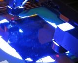
Lithography has become a basic process in wafer processing. In the lithographic process, a photoresist is first uniformly applied to the substrate by spin coating or spraying. With the aid of a structured template, typically a chrome-coated glass mask, the open areas are exposed to UV light or particle irradiation, whereby the solubility of the resist changes. Depending on the resist and process control, a distinction is made between positive and negative resist. In the case of positive resist, exposed areas are released from the developer; in the case of negative resist, the unexposed areas are dissolved during development. After development, the further structuring of the substrate can be carried out by chemical or physical removal.
Lithography

Process Steps
Resist coating
Spin and spray coating for structured 8 "wafers with low and high viscosity positive and negative resists (10 cSt to 5000 cSt) for coating thicknesses from 1.2μm to 60μm.
Exposure:
For exposure, a Maskaligner and a Widefield Stepper are available. Front and back adjustments are possible in the Maskaligner. Exposure can be at proximity distance or as contact exposure. In the Widefield Stepper, a resolution of 0.8μm is possible with a maximum field size of 50 x 50mm².

Development:
The development of the coatings can be carried out both by puddle as well as spray development.
Special resist applications:
Thick resist coatings
Lift-off processes
Equipments
| Equipment | Type | Producer |
| Stepper | FPA-3000 iW | Canon |
| Mask Aligner | MA200 Compact (FSA+BSA) | SUSS |
| Spin Coater | ACS200 PLUS | SUSS |
| SVG90 S | SVG | |
| Spray Coat | ACS200 PLUS | SUSS |
| Developer | ACS200 PLUS | SUSS |
| SVG90 S | SVG | |
| CDSEM | CDSEM9260 | Hitachi |
 Fraunhofer Institute for Silicon Technology