 Fraunhofer Institute for Silicon Technology
Visit our experts at the LASER World of Photonics!
Are you curious about what we will be presenting at this exciting event? Below you will find fascinating information about our innovative exhibits!
Are you curious about what we will be presenting at this exciting event? Below you will find fascinating information about our innovative exhibits!
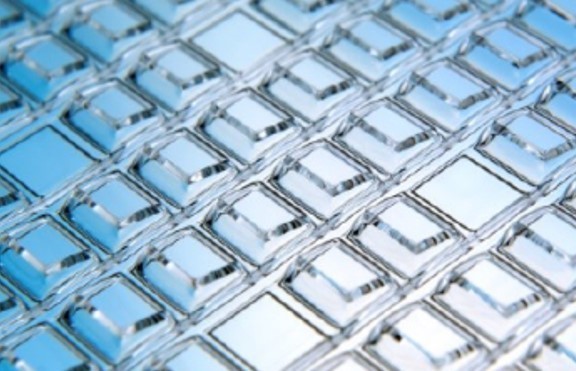
At the trade fair, visitors will receive comprehensive information on hot viscous molding, an innovative process in micro-manufacturing. This process enables the precise production of micro-components by heating viscous materials, which are then molded. Particularly noteworthy is a newly developed process at Fraunhofer ISIT based on the hot viscous molding of glass. With the help of this process, it is possible to structure glass wafers with high aspect ratios at wafer level in such a way that the good optical properties are retained.
With the help of this unique technology, new components can be manufactured from glass at wafer level for the first time that meet the qualitative requirements of optics. This means that microlenses, reflectors and specially shaped optical windows can be produced in large quantities at wafer level without further mechanical processing, enabling cost-effective mass production of micro-optical components (wafers with gold-plated concave mirrors). In combination with MEMS scanners and active optical components, this manufacturing process is the key to hermetically encapsulated MEMS components that meet the high requirements of optical functionality (MEMS mirrors with inclined windows).
Visitors can also find out about the specific steps of the hot viscous molding process, discover application examples in the microelectronics and semiconductor industries and learn about current research projects and innovative developments. In addition, opportunities for cooperation in research projects will be discussed, which could be of great interest to interested partners.
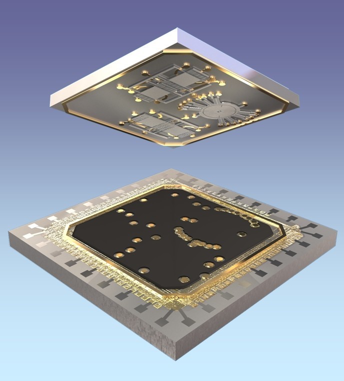
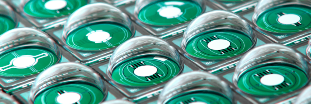
Get to know our advanced wafer-level housing technologies at the trade fair! We use the precision of semiconductor and microsystem technologies to realize robust and compact housings for microsensors, actuators and micro-optical components.
Our team places particular emphasis on hermetic capping and uses various joining technologies, including glass solder and metals. Our housings for micro-optical components offer optically transparent window surfaces for the visible range up to the far infrared. Wafer-level packaging is optimal for post-CMOS processing of customized wafers and is used in areas such as IR sensors, inertial sensors, magnetic field sensors and MOEMS devices.
Visit our booth at the fair and learn more about our solutions and technologies! We are looking forward to your visit!

This year, Fraunhofer ISIT is presenting new developments in the field of piezoelectrically driven MEMS mirrors. Actuation using AlScN enables remarkable mirror deflections and high frequencies in both quasi-static and resonant operation due to the material-specific large driving force and high material elasticity. Furthermore, the MEMS mirrors are characterized by very good deflection-voltage linearity and impressive long-term stability. Thanks to their great design flexibility, Fraunhofer ISIT's MEMS mirrors are suitable for use in a wide range of applications, such as industrial and automotive LiDAR systems, quantum computing and sensing, spectroscopy and optical communication.
Fraunhofer ISIT's LIDAR camera is based on resonant MEMS mirrors and offers an innovative solution for modern requirements in the fields of autonomous driving, drones and 3D object detection.
The laser beam is digitally modulated and photodetection is performed by an APD sensor. The unique design with a specially shaped glass cover minimizes reflections, ensuring a reliable and stable measurement.

Integrated photonics technology has evolved from lab-based optical systems to compact, chip-based solutions. These advances are primarily due to developments in nanofabrication from the MEMS sector, which have driven the commercialization of integrated semiconductor lasers, waveguides, modulators and photodetectors.
A central element of this technology are waveguides, which are used in photonic integrated circuits (PICs) to minimize light losses during fiber connection. At Fraunhofer ISIT, innovative processes are being developed to produce waveguides from materials such as silicon, aluminum nitride and silicon nitride, which offer high efficiency and multifunctionality.
Another focus is on MEMS-modulated PICs that enable precise optical control. With the use of piezoelectric materials such as AlScN, modulated waveguides can be realized for applications in quantum computing and photonic neural networks.
The expertise in the production and characterization of these innovative materials makes Fraunhofer ISIT an important partner in the field of photonic integrated circuits.