Fraunhofer Institute for Silicon Technology
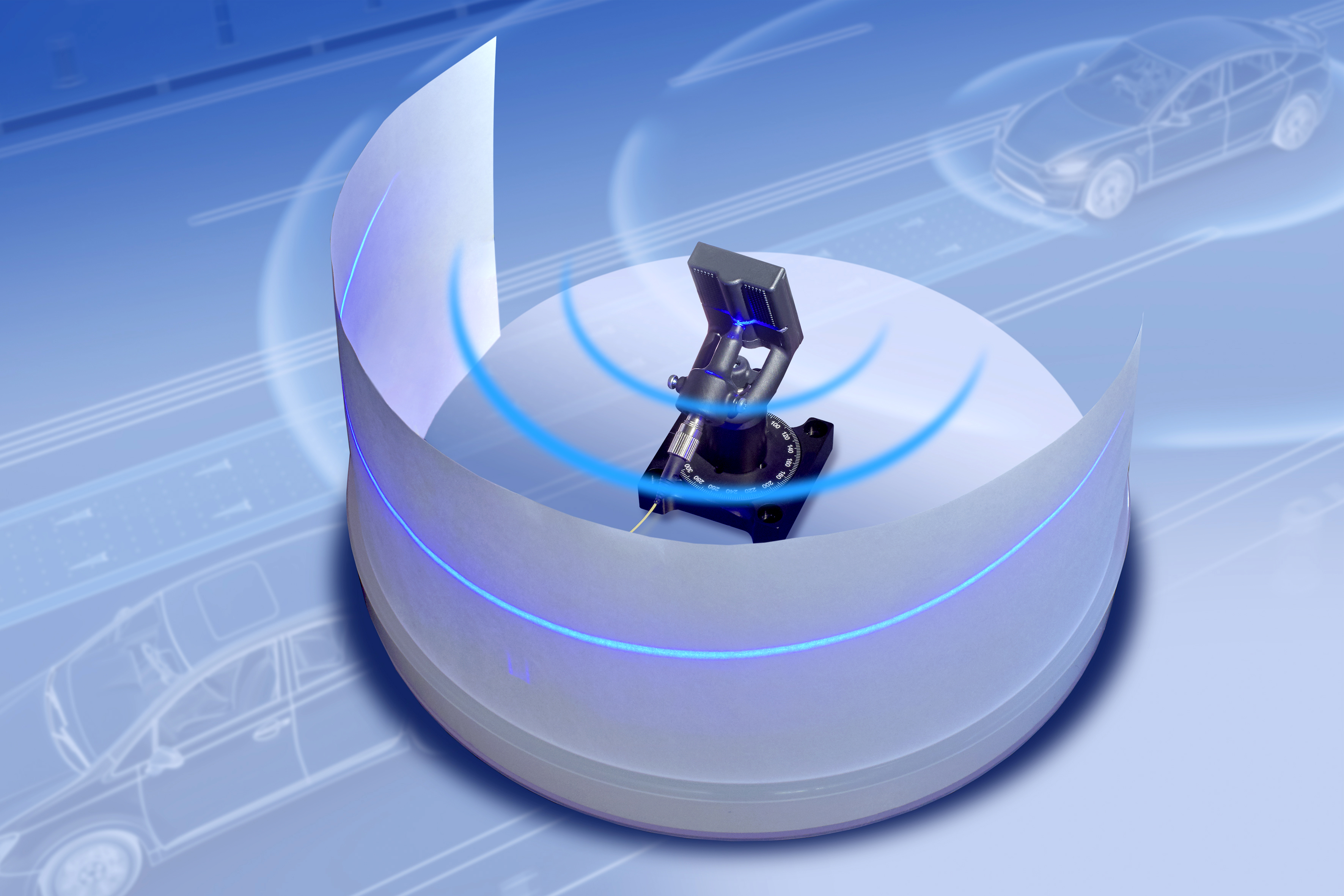
Also this year Fraunhofer ISIT presents itself at Photonics West in San Francisco. Under the heading "Microsystems and their fabrication for optical applications", we will provide information and offers on the research topics of high-power laser scanners, MEMS LIDAR systems, microlenses and mirrors, microlens arrays, as well as energy-efficient and smart sensors for the next generation of autonomous systems.
MEMS applications
High-Power Laser Scanner
High power laser scanner (with stroboscope illumination) Laser material processing, laser welding, laser cutting etc.
The new MEMS scanners developed by Fraunhofer ISIT allow the fast deflection of laser radiation with up to 4.5 kWatt at scan frequencies in the kilohertz range. This allows a significant increase in throughput for many manufacturing processes and, in many cases, new functionality and quality enhancement. Dielectrically coated, highly reflective mirrors with apertures of up to 20 mm are unique worldwide.
MEMS-LIDAR-Systems
LIDAR Systems / 3D Camera
The 3D camera is based on a 2D MEMS scanner that uses the principle of the phase difference of an emitted laser beam to the detected "echo" as a distance measurement. The phase detection algorithm allows 60 million 3D measurements per second. The camera has a resolution of 450 x 450 pixels and delivers six images per second. The depth resolution is said to be a few millimeters and the maximum detectable distance to the object is 2 meters.
Microfabrication process
Opto-Packages
Glass packages for wafer-level packaging
Development of remolded glass wafers to achieve specially adapted optical functions. Based on a glass wafer reshaping technique developed and patented by Fraunhofer ISIT, microlenses, reflectors and specially shaped optical windows can be mass produced at wafer level, enabling low-cost mass production of micro-optical devices. In the context of MEMS scanners and IR MEMS devices, this manufacturing process is the key to hermetically encapsulated MEMS devices with optimal optical functionality.
Microlenses and mirrors, microlens arrays
Lenses and mirrors manufactured from glass at wafer level.
The process is particularly suitable for the production of precision optics with high uniformity and reproducibility. The hot viscous molding process can now also be used to produce aspherical optics for optical and IR applications.
Neurosmart project
Neurosmart - Sensors learn to think
In the Fraunhofer-Gesellschaft's lead project NeurOSmart, five institutes (ISIT, IPMS, IMS, IWU, IAIS) under the leadership of ISIT are jointly researching particularly energy-efficient and intelligent sensors for the next generation of autonomous systems. In the process, the bridges between perception and information processing are being redefined by innovative electronics.
The human brain serves as a model for the so-called neuromorphic electronics to be developed, as it is very energy-efficient when making decisions despite its enormous computing power. This type of data processing is realized by a new type of analog computer memory technology, which is also capable of performing arithmetic operations when data is newly acquired in the system. The advantages of the new approach are underlined by the parallel development of particularly small and efficient models for object recognition and classification, which are specifically adapted to the sensor, the new possibilities of directly integrated electronics and their applications.
Currently, this approach is being combined for the first time with a complex LiDAR (Light Detection And Ranging) system developed at Fraunhofer and tested in an application-oriented environment.
Visit us at Moscone Center, Booth 4029.