Extended cooperation: CEA-Leti and Fraunhofer advance memory technologies for EU Chips Act
TOWARDS ENERGY-SAVING CHIPS FOR DIGITAL, ANALOG AND RF
CEA-Leti and Fraunhofer are planning to extend their collaboration in the development and integration of novel memory technologies based on ferroelectric materials within the scope of the recently announced FAMES Pilot Line (https://fames-pilot-line.eu/), a pioneering project aimed at advancing semiconductor technologies in Europe. This initiative aligns with the ambition of the EU Chips Act, which seeks to bolster EU semiconductor capabilities and ensure technological sovereignty.
The pilot line will develop five new sets of technologies:
- FD-SOI (with two new generation nodes at 10nm and 7nm),
- Several types of embedded non-volatile memories (OxRAM, FeRAM, MRAM and FeFETs),
- Radio-frequency components (switches, filters and capacitors),
- Two 3D integration options (heterogeneous integration and sequential integration), and
- Small inductors to develop DC-DC converters for Power Management Integrated Circuits (PMIC).
The five new technologies will create market opportunities for low-power microcontrollers (MCU), multi-processor units (MPU), cutting-edge AI and machine learning devices, smart data-fusion processors, RF devices, chips for 5G/6G, chips for automotive markets, smart sensors and imagers, trusted chips and new space components. “By integrating and combining a set of cutting-edge technologies, the FAMES Pilot Line will open the door to disruptive system-on-chip architectures and provide smarter, greener and more efficient solutions for future chips. The FAMES project will indeed pay special attention to semiconductor sustainability challenges,” – said Jean-René Lèquepeys, CTO of CEA-Leti.
The pilot line will be accessible to all EU stakeholders (universities, RTOs, SMEs and industrial companies) and all like-minded countries through annual open calls and upon request, following a fair and non-discriminatory selection process. The project will benefit from funding that will be provided in equal parts by participating member states and the Chips JU. “The Chips Joint Undertaking (Chips JU) is proud to contribute to this strategic initiative and strengthen the EU’s sovereignty in a critical domain. This pilot line will advance essential semiconductor technologies, while maintaining a strong focus on sustainability, and foster the collaboration between several European actors. The Chips JU aims to act as a catalyst and a model for further public and private collaborations in key areas,” explained Jari Kinaret, the Chips JU executive director.
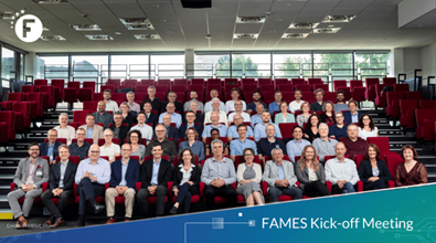
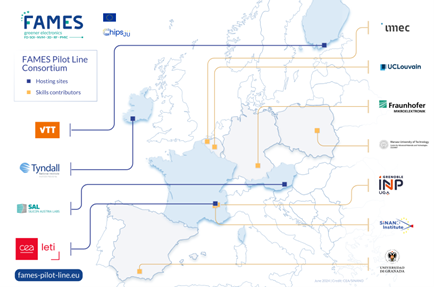
The FAMES consortium brings together an outstanding group of partners:
- the pilot line coordinator, CEA-Leti (France),
- imec (Belgium),
- Fraunhofer (Germany),
- Tyndall (Ireland),
- VTT (Finland),
- CEZAMAT WUT (Poland),
- UCLouvain (Belgium),
- Silicon Austria Labs (Austria),
- SiNANO Institute (France),
- Grenoble INP-UGA (France),
- University of Granada (Spain).
Within the envisaged Fraunhofer contribution to the pilot line three of its institutes are bringing in their expertise:
Fraunhofer Institute for Photonic Microsystems IPMS, with its Center Nanoelectronic Technologies (CNT)
At the Center Nanoelectronic Technologies, Fraunhofer IPMS conducts applied research on 300 mm wafers for microchip producers, suppliers, equipment manufacturers and R&D partners. Research includes topics such as 300 mm Front-end technology modules, test chips, energy storage and next generation memory technology. In this cooperation, Fraunhofer IPMS will bring its unique experience on the HfO2 ferroelectric material optimization, stack benchmarking, module development and device optimization whereas CEA-Leti brings a unique pilot-line enabling the integration of FeRAM or FeMFET on top of CMOS wafers down to the 22nm node, which is adapted for dense and 300mm large-scale memory arrays, which are used for energy-efficient AI accelerators.
Fraunhofer Institute for Silicon Technology ISIT
Fraunhofer ISIT is developing advanced Post-CMOS and III-V devices and systems in its 200 mm cleanroom. These span the application range from MEMS, via micro- to power electronics. Previously, ferroelectric AlScN thin films have been discovered at Fraunhofer ISIT and BEOL-FeFETs were successfully processed. As part of this activity, novel nitride-based ferroelectric materials are being established and evaluated for their integration in CMOS memory benchmark vehicles. Beyond the memory stack processing, ISIT will also conclude the BEOL CMOS processing. The aim is a thorough evaluation of nitride-based FeRAM that promise extreme retention (>100 years, >500°C).
Fraunhofer Institute for Reliability and Microintegration IZM, with its All Silicon System Integration Center Dresden (ASSID)
Fraunhofer IZM’s focus is on packaging technology and the integration of multifunctional electronics into systems. Within the pilot line its department "Wafer Level System Integration" (WLSI) especially at ASSID will develop and employ advanced packaging and system integration technologies for emerging memory technologies on 300 mm wafers in 2.5 and 3D stacks. Additionally, its department for Environmental & Reliability Engineering will evaluate todays and tomorrow’s memory technologies and their integration approaches towards their sustainability. From environmental and sustainable perspective system solutions based on ferroelectric memories offer advantages compared to state-of-the-art solutions because of the low power switching capabilities enhance life cycle of devices and widening the application portfolio of self-powered systems. Further, the low switching voltage compared to conventional floating gate storage contributes to significant chip area reduction and therefore reduction of energy, chemistries and raw materials in chip fabrication process. Such improvements in chip area and power will be monitored and benchmarked within the cooperation.
A European consortium under the coordination of the Research Fab Microelectronics Germany (FMD for its acronym in German) intends to establish over the next few years the most comprehensive and cutting-edge pilot line for “Advanced Heterogeneous System Integration” as a contribution to the implementation of the EU Chips Act. The participation of CEA-Leti and other European partners in the aforementioned pilot line will be similar to the involvement of the Fraunhofer institutes IPMS, IZM and ISIT in the FAMES pilot line. The aim of these efforts is to ensure a close link between the content of the upcoming pan-European pilot lines.
 Fraunhofer Institute for Silicon Technology
