 Fraunhofer Institute for Silicon Technology
Establish a reproducible thick wire bonding process for contacting power MOSFETs on FR4 substrates.
In order to extend the know-how on the topic of thick wire bonding of power semiconductor devices on FR4 substrates at ISIT, a feasibility study for a thick wire bonding process with 500µm Al thick wire was carried out as part of a microtechnologist's final thesis. Shear tests and cross-section analyses were used to evaluate the bonded joints for shear strength and crack formation.
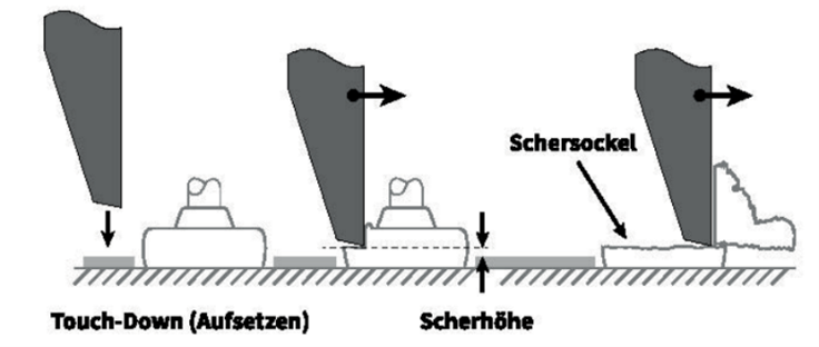
Shear tests
A shear test is a destructive method for the analysis of bonded joints (e.g. bare dies bonded or soldered to substrates, soldered SMD components, bump or bond wire joints). In this process, a shear bit travels horizontally against the sample at a predefined height and speed and shears it. During the shearing process, the force is recorded. For clarification, the shear sequence of a gold bump is shown in the following illustration from left to right (Figure 1)., Wedge joints are tested in the same way.
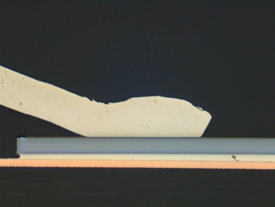
Cross section analysis
Metallographic microsection preparation is another destructive examination method. Here, material-specific properties such as grain boundary alignment or the formation of the intermetallic phase of microstructures as well as, in the case of damage, cracks inside components, solder joints, or defective contact bonding of components are examined. For this purpose, the samples are embedded in synthetic resin, ground and then polished so that the sample can then be analyzed under an optical microscope. An example of such a sample is shown in the adjacent figure (Fig.2).
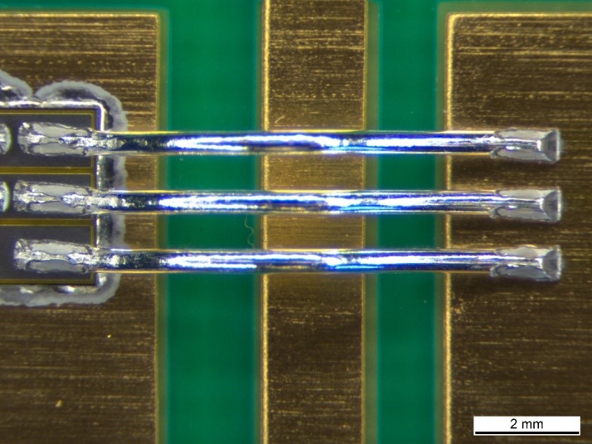
Result
To find a suitable parameter set, the bonding parameters were increased or decreased depending on the shear results. After several bonding runs with different parameters, a suitable parameter set was determined with which it is possible to realize a good bonding result with a shear strength above 35MPa as well as a continuous bond to the connection pads for test abutments. The following picture (Fig.3) shows a series of bondings which meet the required qualitative demands.
Conclusion
The knowledge gained in the course of this work will help in the future evaluation of thick-wire bonded structures. Above all, it has been possible to develop a bonding program that can be used as a basis for future applications and adapted to the application in question by modification.
ISIT offers technology consulting and support for process evaluation and optimization. We are at your disposal for individual questions.