Fraunhofer Institute for Silicon Technology
Frank Dietz
New Equipment for the development of vertical gallium nitride power devices
The Group for Advanced Power Transistors at Fraunhofer ISIT develops new types of power devices. For decades, these power devices have used silicon (Si) as semiconductor material. A few years ago, our group started investigations on using gallium nitride (GaN) for manufacturing semiconductor devices. The reasons for using this wide band gap material are the superior properties of GaN, such as a higher switching speed and an improved RDS(on)/VBR(DSS) – ratio, compared to silicon. In the Fraunhofer project “Vertigo” GaN based diodes and transistors are developed. During the project, our knowledge, technology and equipment for processing silicon based power devices will become the working platform for processing the new material.
In this article, we give a short status report about the procurement of further specific equipment for GaN processing that is founded by the “Research Fab Microelectronics
Germany”.
One step further
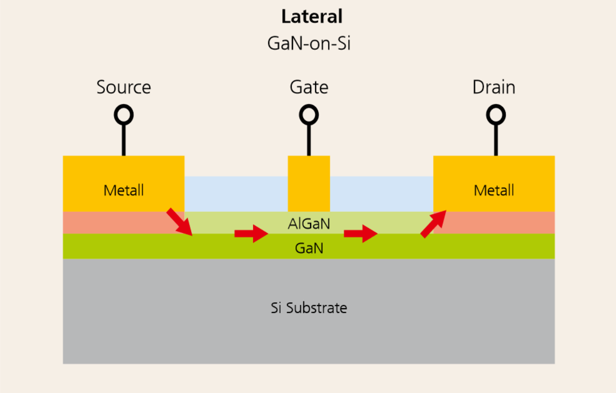
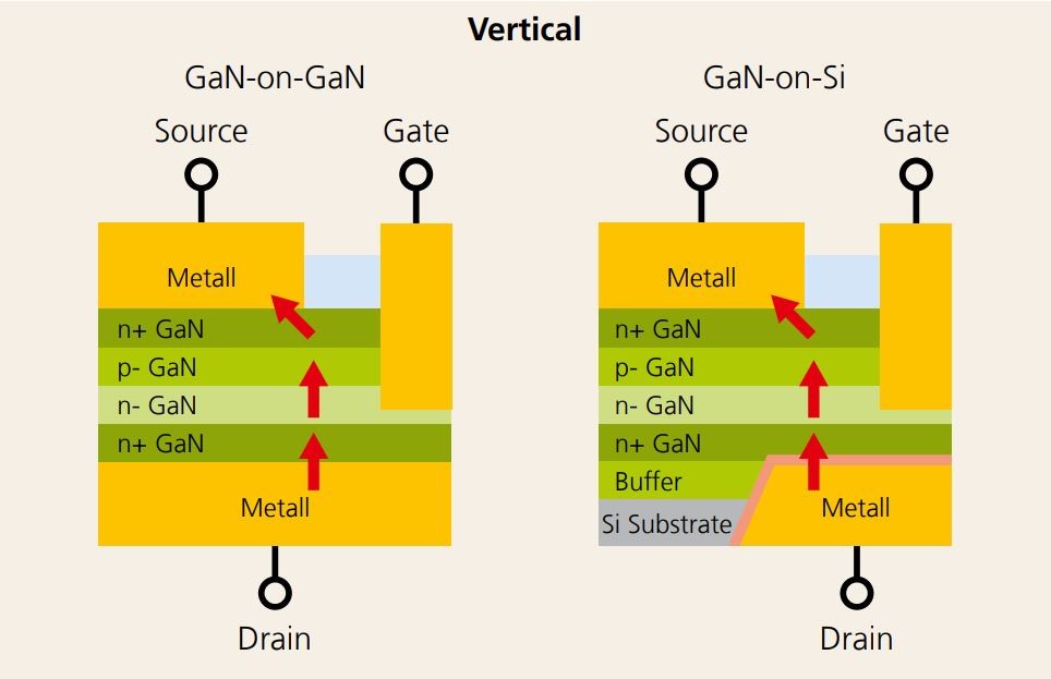
State of the art GaN devices are lateral HEMTs (high electron mobility transistor) using the 2D electron gas effect (see figure 1a). The primary goal is to release the full potential of GaN based diodes and transistors by vertical device structures (see figure 1b). In order to satisfy the demand for mass market suitability, the 200 Volt devices are developed and manu- factured on a 200 mm platform available at ISIT. The wafer material consists of 3 layers: a buffer layer for atomic lattice matching deposited on a Si carrier wafer (with a (111) surface), followed by a functional GaN based layer system. The 200 mm substrates with epitaxial layers are purchased from external suppliers and processed in the ISIT clean room.
Additional equipment at ISIT for new GaN device platform
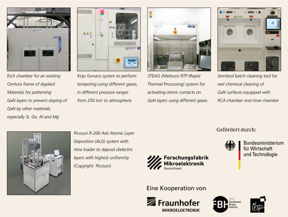
A technology platform for power devices based on the III-V semiconductor material gallium nitride (GaN) is being established at the Fraunhofer ISIT. The development and processing of new power devices based on GaN epitaxy on 200 mm (111) silicon wafers takes place in the clean room at Fraunhofer ISIT, which is originally equipped and used for Si-based micro-electro-mechanical systems (MEMS) such as sensors, scanning micro mirrors and piezoelectric systems. For the development of vertical GaN devices, the existing technology park will be expanded with new equipment and processes. The additional equipment was procured as part of the project „Research Fab Microelectronics Germany”, funded by the German Federal Ministry of Education and Research. It will enhance ISIT’s capabilities in dry and wet etching, cleaning, tempering and rapid thermal processing as well as the electrical characterization of manufactured components. Most of the systems are already installed and in use. The new equipment primarily serves to prevent contamination of GaN by Si and adds key processes for GaN based devices that will lead towards innovative research and development projects. With this perspective, Fraunhofer ISIT is as well enhancing device measurement capabilities for static and dynamic wafer and device testing for the new III-V semiconductors.