Dr.-Ing. Thomas Knieling, Dr.-Ing. Shanshan Gu-Stoppel, Dr. Wolfgang Reinert, Hans-Joachim Quenzer
MEMS processes for Quantum Computing and Quantum Sensing
TechBlog /
Since 1994 Fraunhofer ISIT is one of the leading institutes in Europe for applied research in MEMS development and processing. Products like MEMS mirrors, loudspeakers, bio sensors and microfluidics have been manufactured in the ISIT cleanroom fab (2500 m², 8” / 200 mm silicon and crystalline quartz / amorphous glass wafers). Moreover, transistors and batteries for power electronics applications are being developed in our own facilities. Both MEMS and power electronics have been successfully transferred into prototypes and products.
Fraunhofer ISIT provides an extensive process and technology portfolio (fig. 1). Several products and applications have been realized in industrial and public research collaborations.
MEMS Processes and Technologies
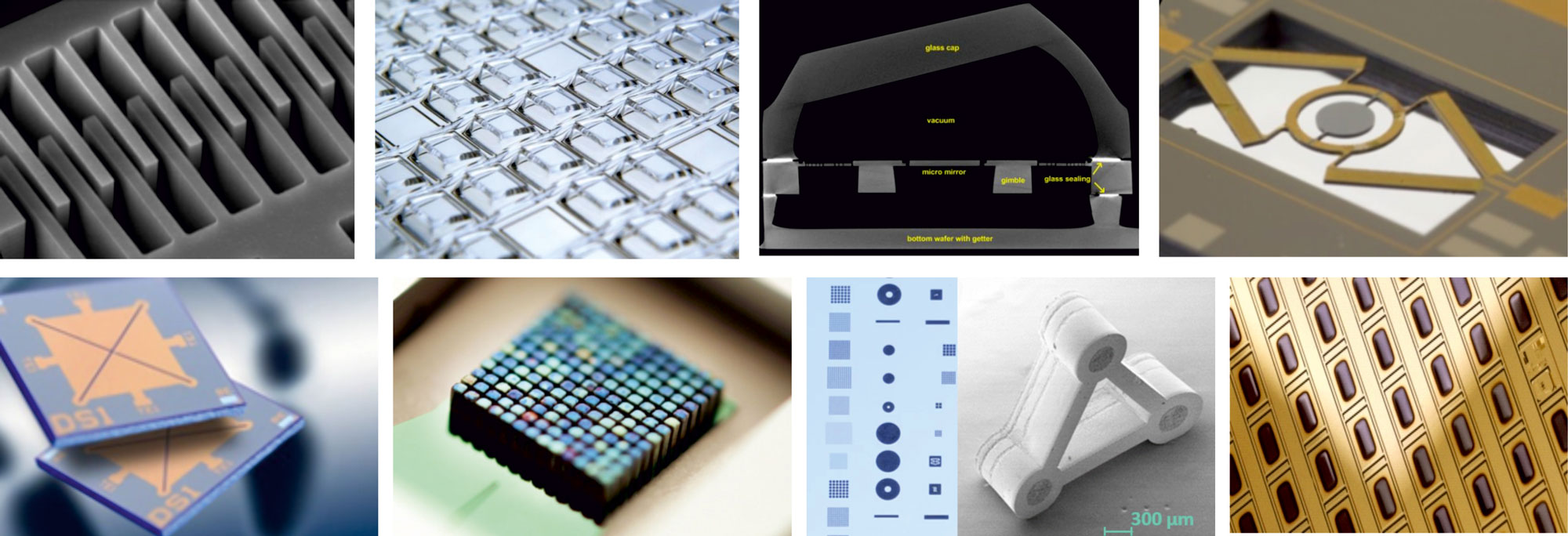
3D Glass forming: Optical vacuum packages for MEMS encapsulation
The ISIT patented 3D glass forming technology enables the production of several optical components like lenses, mirrors, prisms etc. accompanied with hermetic optical packaging and getter integration for getting and maintaining high vacuum (fig. 2).
Moreover, by adding special dielectric coatings it is prepared for UHV applications, for instance for ion trap applications.
Piezo Technology based on PZT, AlN & AlScN
ISIT has long term experience with PZT (e3,1 = -12 1C/m²) sputtering or evaporation. However, ROHS restrictions, material degradation and monopolar characteristics of PZT have led to new developments using sputtered AlN or AlScN with e3,1 = -1C/m² for AlN and -2,4C/m², respectively.
Module Services: Miniaturized Laser Sources
Based on our MEMS wafer processes, we developed a modular glass-/silicon packaging platform for heterogeneous integration of optical components [1]. The glass capping provides a hermetic side looking window in this example. The assembly and wire bond interconnection can be performed on single substrates, panels and on an up to 200 mm wafer.
Silicon provides the required stability of an optical bench. A precision assembly machine configured with in-situ laser soldering and active lens adjust provides the required infrastructure to realize new optical constructions and produce demonstrators, such as a multi-channel laser light source (fig. 3).
MEMS Product Application Examples
MEMS Optical Micro Mirrors
Besides our long term proven resonant mirror technology our new piezo actuator design (Fig. 4) and technology extends the application space substantially [4, 5].
Tab. 2 shows the main parameter space where however due to physical restrictions these parameters cannot be combined arbitrarily.
Parameter
Min.
Max.
Frequency / Hz
100 / quasistatic
100000
Optical scan angle (FOV) / °
0,01
40
Aperture / mm
0,2
20
Tab. 2: Main parameters for quasistatic mirrors.
Besides tilting motions with this four electrode/actuator architecture also translational or mixed mirror motions can be performed, all precisely defined in a closed-loop scheme through very accurate optical or piezoelectric position sensing. Simulations have shown that already with this first, non-optimized design large hubs up to 200 µm can be reached (fig. 5).
Possible Applications can be the compensation of external motion in the optical or atom beam paths in gravimeters based on atom interferometry.
References
[1] V. Stenchly et al., Modular packaging concept for MEMS and MOEMS. DOI.
[2] W. Reinert, A miniaturized RGB-laser light engine. DOI.
[3] S. Gu-Stoppel et al.: A triple-wafer-bonded AlScN driven quasi-static MEMS mirror with high linearity and large tilt angles. DOI.
[4] S. Gu-Stoppel et al.: A designing and manufacturing platform for AlScN based highly linear quasi-static MEMS mirrors with large optical apertures. DOI.