Multi-functional hermetic sealing with combined Glass/Si packages

Research & Development

© Fraunhofer ISIT
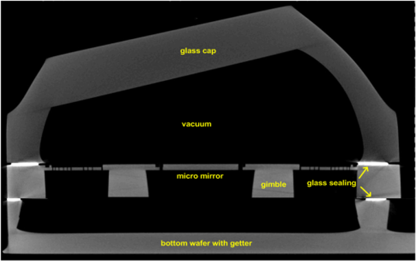
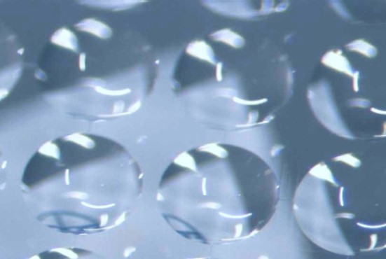
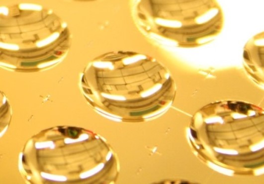
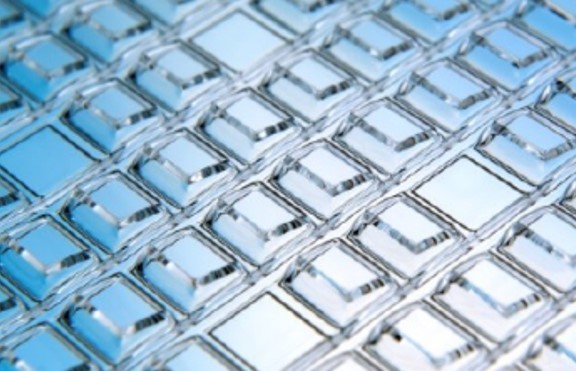
Glass-Si composite Wafer

The basis for our hermetic glass capping is our patented glass flow technology. Combined Silicon and glass substrates as well as several etch and patterning technologies come here into play.

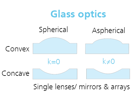
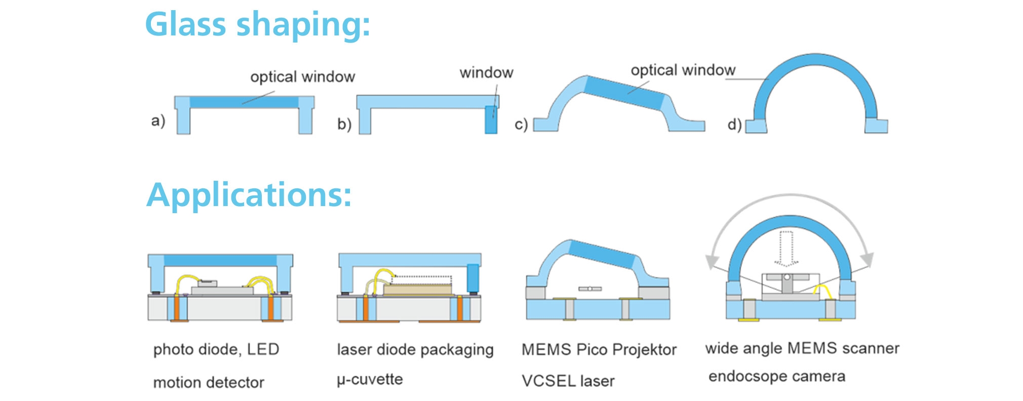
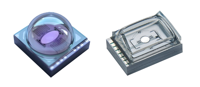
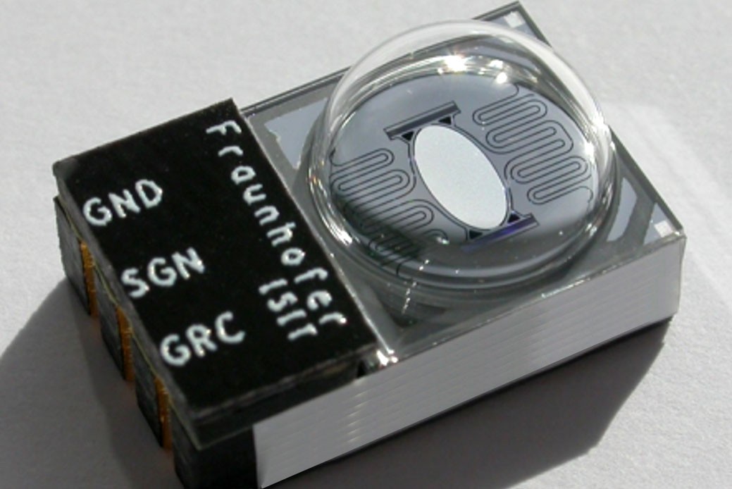
With this technology we manufacture new components made of glass at wafer level. Without further processing we now can manufacture micro lenses, reflectors, prisms and other specially shaped optical windows or parts in large numbers at wafer level. This enables an economical low/high volume production of micro optical components for your application.

© Fraunhofer ISIT
CT image of WL sealed micro mirror

3D-Glass Forming: Optical vacuum packages for MEMS encapsulation

The ISIT patented 3D glass forming technology enables the production of several optical components like lenses, mirrors, prisms etc. accompanied with hermetic optical packaging and getter integration for getting and maintaining high vacuum. Moreover, by adding  getter coatings it used at low pressures of 10-8 mbar. For lower pressures (UHV) like in ion traps more R&D efforts have to be made like adding dielelectic coatings and higher qualification.

© Fraunhofer ISIT


Ø APERTURE [mm]

Material

Application

Lens

Mirror

VIS

0.4 - 8.0

2.0 - 8.0

glass

Sensors, Imager

NIR

0.3 - 0.8


glass, Si

LD Beamshaping

FIR

0.5 - 1.2

2.0 - 16.0

Si

FIR Sensor & Imager

UPDATE | 03.02.2022

© Kiutra GmbH
Fig. 1: Temperature curve that affected the mirror packages.
© Fraunhofer ISIT
Fig. 2: Tested mirror packages with hermetically integrated micromirrors (the mirror diameters are 2 mm x 4 mm on the left and 1 mm on the right).

The generation and use of QuBits e.g. in superconducting or ion trap based QC systems usually require very low temperatures of some 100 mK to some K, otherwise the states decay too fast (decoherence) and cannot be used for computational operations or their accuracy is below the error tolerance. Our hermetic glass packages must therefore also withstand these temperatures and were therefore carried out at our partner, Kiutra GmbH, in their novel cryostats based on adiabatic cooling by demagnetization. Fig. 1 shows the temperature curve.


A very positive result is that our standard mirror packages with inclined and dome shapes (Fig. 2) survived this stress without damage. The vacuum was still present in each case and the micromirrors in the packages oscillated in an identical manner after the tests as before.

This result complements our portfolio with technologies also for ultracold applications.

Silicon Optics

Privacy warning

With the click on the play button an external video from www.youtube.com is loaded and started. Your data is possible transferred and stored to third party. Do not start the video if you disagree. Find more about the youtube privacy statement under the following link: https://policies.google.com/privacy

Our innovative glass flow technology is good for silicon optics. The process benefits from standardized procedures of structuring silicon in a clean room. Lear more about this process by watching our video. 

Overview

Characteristics

  • Filling of deep silicon structures by amorphous glass
  • CTE glass = CTE silicon
  • Through vias or blind holes
  • Aspect ratio 4-5
  • Glass types: Borofloat 33, AF32

USPs

  • Glass structures in silicon or vice versa
  • Positive properties of glass and silicon combined: CTE match, electric properties
  • Glass: Dielectric material, HF suitable, transparent
  • Silicon: High thermal conductivity

Application

  • Optical packaging, photonic circuits, optical signal manipulation for quantum sensing (gravimetry, spectroscopy, etc.)
  • Optical (glass in Si) or electrical (metal in glass) feedthroughs, for instance for ion traps.

References

  1. V. Stenchly et al., Modular packaging concept for MEMS and MOEMS, doi:10.1088/1742-6596/922/1/012015
  2. S. Gu-Stoppel et al.: A triple-wafer-bonded AlScN driven quasi-static MEMS mirror with high linearity and large tilt angles; doi: 10.1117/12.2542800
  3. S. Gu-Stoppel et al.: A designing and manufacturing platform for AlScN based highly linear quasi-static MEMS mirrors with large optical apertures; doi: 10.1117/12.2583399