Multi-Channel Laser Light Source

Research & Development

© Fraunhofer ISIT
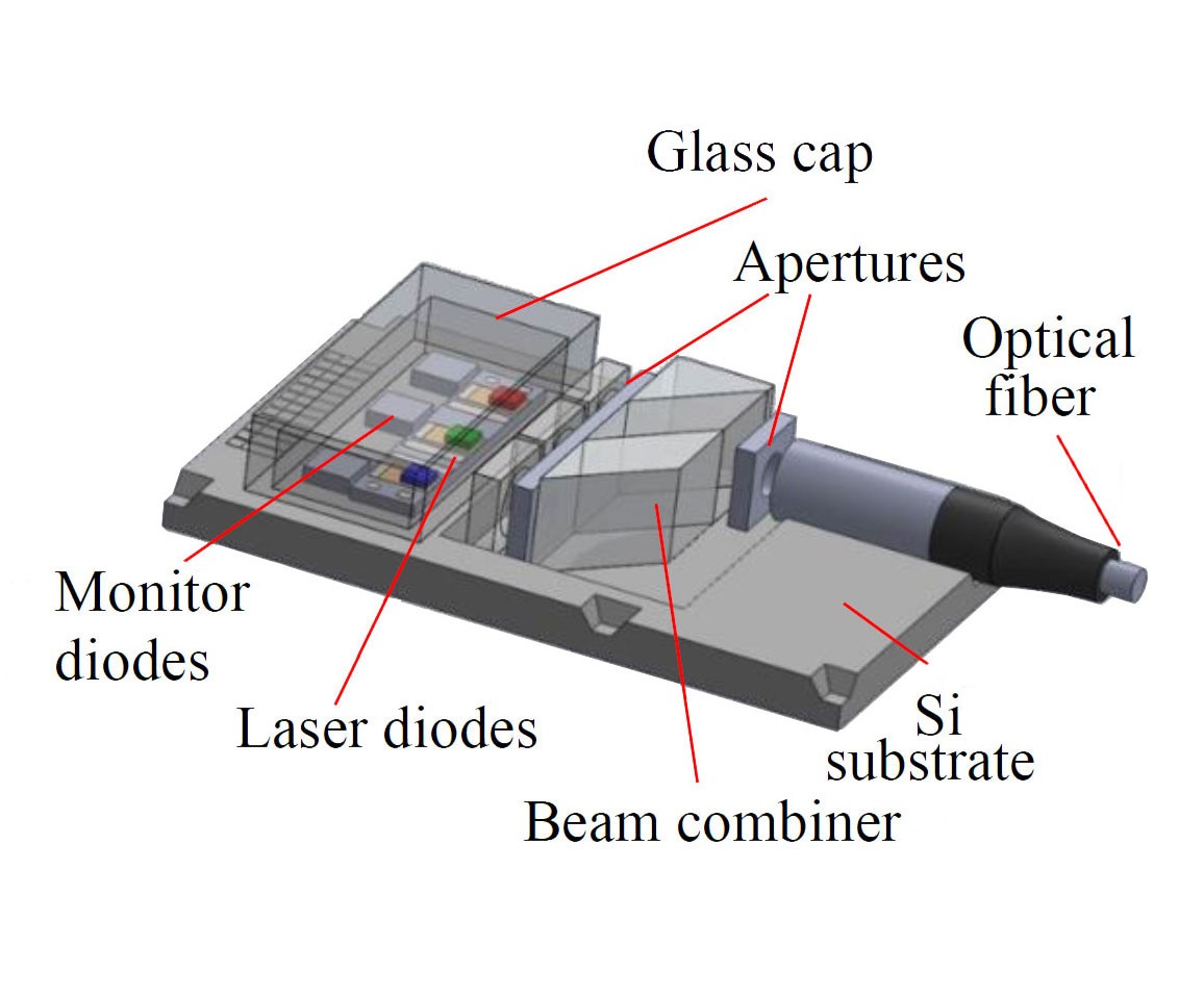
A multi-channel RGB laser light source based on optical glass-silicon packaging platform.

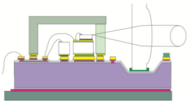
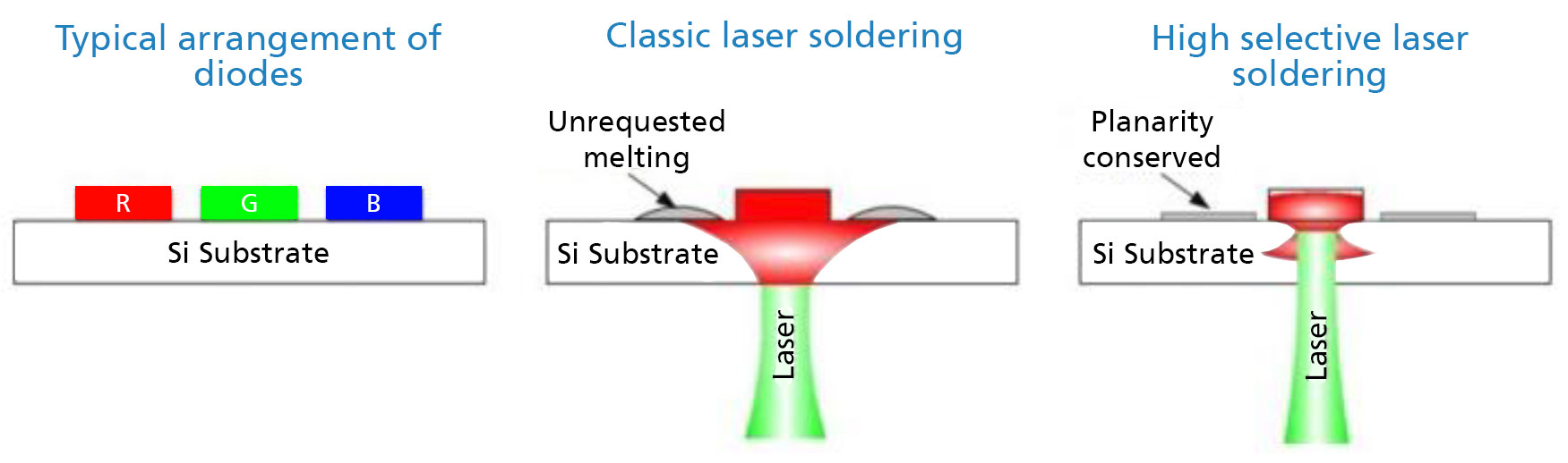
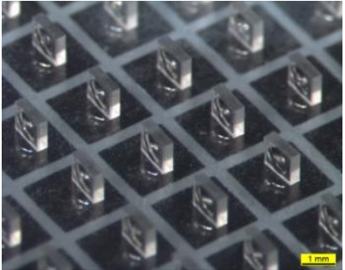
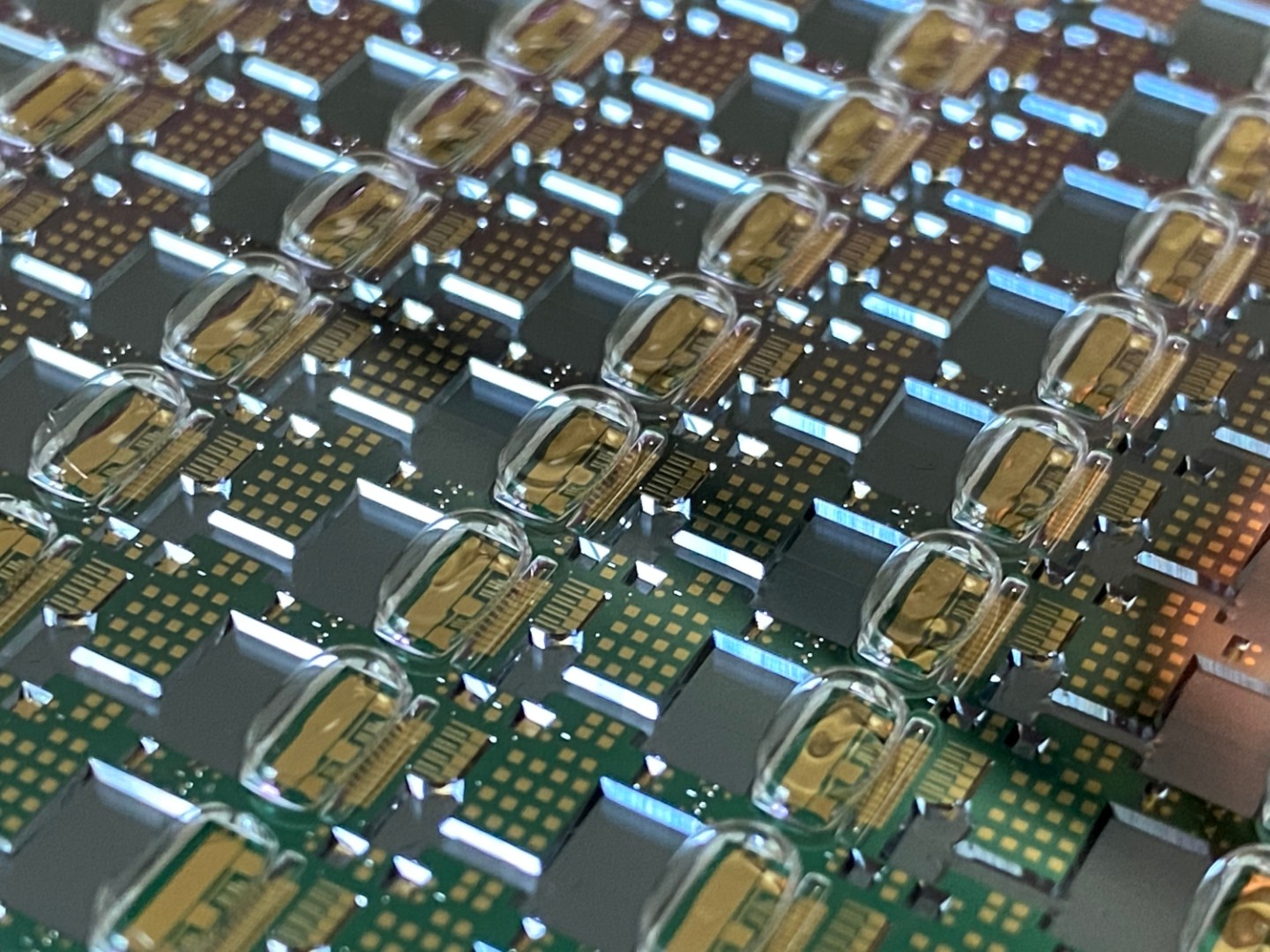
Based on our MEMS wafer processes, we developed an optical bench silicon chip where all laser components and the diode laser chips are assembled. For diode chips we use a specially developed solder process with low thermal impact. The assembly and wire bond interconnection can be performed on single substrates, panels and 200 mm wafer.

Silicon here provides the required stability of an optical bench. A precision assembly machine configured with in-situ laser soldering and active lens adjust provides the required infrastructure to realize new optical constructions and produce demonstrators, such as a multi-channel laser light source.

Characteristics

© Fraunhofer ISIT
Wire bonding of the module on a PCB. Since each source has its own characteristics, different adjustments should be made for each channel.
  • Multi-channel miniaturized laser light source (silicon-based optical bench)
  • Modular glass-silicon packaging platform for heterogeneous integration of optical components 
  • Glass capping provides a hermetic side looking window 
  • Si substrate provides required stability of an optical bench

USPs & Benefits

© Fraunhofer ISIT
Assembled Molded micro-square plane-convex glass lenses (f = 1.39 mm)
  • Possibility of heterogeneous integration of optical components by a modular glass-silicon packaging platform
  • Hermetic side viewing window provided by glass cover
  • Required stability of an optical bench by silicon substrate
  • Ability to perform assembly and wire bonding on single substrates and panels and on wafers up to 200mm in size

In addition to wafer technologies, ISIT offers a whole range of services at module level. These range from special processes at chip level, to the production of modules in an industrial manufacturing environment, to the investigation of their reliability under accelerated ageing.

Thanks to state-of-the-art analysis methods such as high-resolution computer tomography, ISIT is known for its fast and reliable failure analyses of industrial production problems and field returns.

Application

© Fraunhofer ISIT
Optical bench chip with Au/Sn solder pads; chip size: 6.8 mm x 7 mm x 0.7 mm
  • Multi atom excitation
  • Manipulation or diverse laser cooling, for instance in ion traps or superconductive units

References

  1. Stenchly et al., Modular packaging concept for MEMS and MOEMS, DOI
  2. Reinert, W., A miniaturized RGB-laser light engine, DOI.