SPIE Photonics West 2025

Visit our experts at SPIE Technology West!

Are you curious about what we will be presenting at this exciting event? Below you will find fascinating information about our innovative exhibits!

Our researchers will be presenting the following topics at SPIE Technologie West in January:

TOPIC AREA
3D glass flow technology
Innovative housing technologies for microcomponents
Resonant and quasi-static MEMS mirrors
MEMS borescope unit (MEMS BORO)
Acoustic surface waves (SAW)
Ultrasonic transducers (PMUTs)
Talk: MEMS mirror-based SPAD LiDAR system
Talk: MEMS Scanner


You can also look forward to exciting conference presentations by two of our scientists!

Be part of this exciting discovery tour into the future of technology!

Micro-Manufacturing

© Fraunhofer ISIT

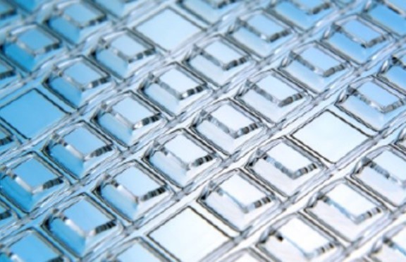
At the trade fair, visitors will receive comprehensive information on hot viscous molding, an innovative process in micro-manufacturing. This process enables the precise production of micro-components by heating viscous materials, which are then molded. Particularly noteworthy is a newly developed process at Fraunhofer ISIT based on the hot viscous molding of glass. With the help of this process, it is possible to structure glass wafers with high aspect ratios at wafer level in such a way that the good optical properties are retained.


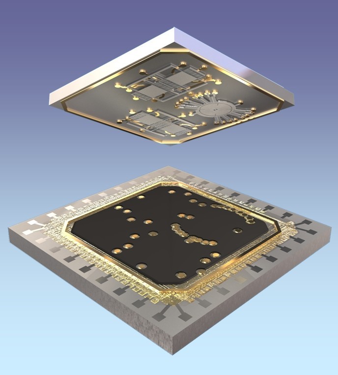
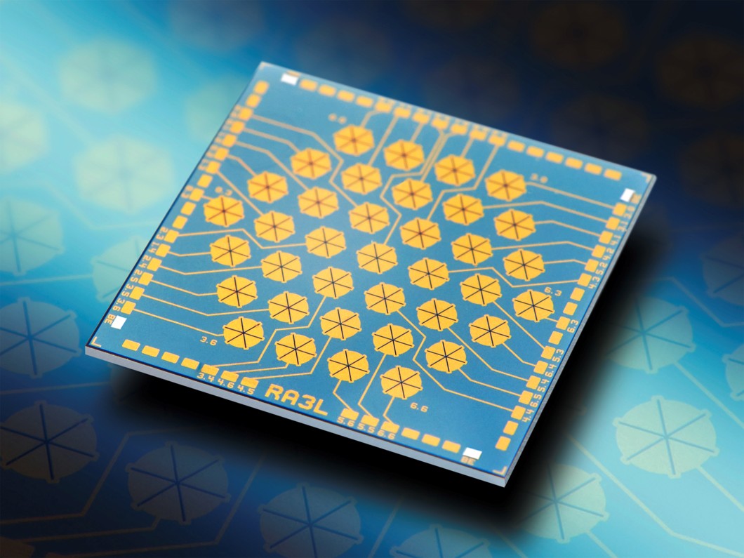
With the help of this unique technology, new components can be manufactured from glass at wafer level for the first time that meet the qualitative requirements of optics. This means that microlenses, reflectors and specially shaped optical windows can be produced in large quantities at wafer level without further mechanical processing, enabling cost-effective mass production of micro-optical components (wafers with gold-plated concave mirrors). In combination with MEMS scanners and active optical components, this manufacturing process is the key to hermetically encapsulated MEMS components that meet the high requirements of optical functionality (MEMS mirrors with inclined windows).

Visitors can also find out about the specific steps of the hot viscous molding process, discover application examples in the microelectronics and semiconductor industries and learn about current research projects and innovative developments. In addition, opportunities for cooperation in research projects will be discussed, which could be of great interest to interested partners.

More Info

© Fraunhofer ISIT

Get to know our advanced wafer-level housing technologies at the trade fair! We use the precision of semiconductor and microsystem technologies to realize robust and compact housings for microsensors, actuators and micro-optical components.

Our team places particular emphasis on hermetic capping and uses various joining technologies, including glass solder and metals. Our housings for micro-optical components offer optically transparent window surfaces for the visible range up to the far infrared. Wafer-level packaging is optimal for post-CMOS processing of customized wafers and is used in areas such as IR sensors, inertial sensors, magnetic field sensors and MOEMS devices.

Visit our booth at the fair and learn more about our solutions and technologies! We are looking forward to your visit!

More info

MEMS Applications

© Fraunhofer ISIT

This year, Fraunhofer ISIT is presenting new developments in the field of piezoelectrically driven MEMS mirrors. Actuation using AlScN enables remarkable mirror deflections and high frequencies in both quasi-static and resonant operation due to the material-specific large driving force and high material elasticity. Furthermore, the MEMS mirrors are characterized by very good deflection-voltage linearity and impressive long-term stability.  Thanks to their great design flexibility, Fraunhofer ISIT's MEMS mirrors are suitable for use in a wide range of applications, such as industrial and automotive LiDAR systems, quantum computing and sensing, spectroscopy and optical communication.

© Fraunhofer ISIT

As part of the BMWK project “MEMS-BORO”, a MEMS-based, miniaturized borescope is being developed for the inspection of highly stressed components in aircraft engines.  The integration of a 3D LiDAR camera into the borescope enables the inspection of previously unattainable component areas. The automated data evaluation to be developed recognizes defects and can classify them, which is why the degree of automation of the currently still completely manual engine inspection process can be significantly increased.

This year, we are presenting the demonstrator of the MEMS borescope unit for the first time at our stand at SPIE Photonics West.


More Info

© Fraunhofer ISIT

Fraunhofer ISIT develops sensors based on the modulation of surface acoustic waves (SAWs). These sensors can be used to measure various physical phenomena: In addition to mass absorption, elastic, viscoelastic or electrical effects can also be utilized. Dedicated functional layers enable a wide range of applications with pressure, humidity, electric field, vibration, gas, bio or magnetic field/current sensors.

The special feature of the SAW sensor technology at ISIT is that it is not based on monocrystalline piezoelectric substrates and is instead manufactured using CMOS and MEMS-compatible silicon technology. This is only possible thanks to the use of the high-performance piezoelectric thin-film material AlScN. In addition to high technology compatibility, other advantages include greater process flexibility with regard to the integration of functional layers, a reduced chip size and the possibility of combining different sensors on one chip.


More Info

© Fraunhofer ISIT

Fraunhofer ISIT develops highly miniaturized piezoelectric micromechanical ultrasonic transducers (PMUTs) for a variety of technical applications, such as distance measurement, gesture recognition, haptic feedback or medical imaging. Depending on the target frequency and application, the concept is based on actuators or membranes made of the piezoelectric high-performance materials AlN, AlScN and PZT, which enable very high sound pressure levels and sensitivities. In this way, efficient ultrasonic transducers with center frequencies of a few kHz up to several hundred MHz can be realized. Production using semiconductor technology enables both high miniaturization and cost-efficient production in large quantities.


More Info

Conference presentations

© Fraunhofer ISIT

In her conference presentation entitled “Piezoelectric MEMS mirror based SPAD LiDAR system enabling real-time monitoring across large covered areas for smart factory applications”, Dr. Jeong-Yeon Hwang will present the MEMS mirror based SPAD LiDAR system developed as part of the Fraunhofer lead project “NeurOSmart”.

The target application of the presented LiDAR system is the monitoring and control of human-robot interaction in smart factories.

Further information on the lead project can be found here:

Neurosmart

© Fraunhofer ISIT

In the presentation entitled “Quasi-static MEMS scanners for an integrated cavity in a trapped ion quantum computer”, Paul Raschdorf introduces the technology of piezoelectrically operated quasi-static MEMS scanners. As an enabling technology in the field of quantum computers, he describes the changes that need to be made in order to adapt the MEMS scanner to the special conditions and new quality measures.

Further information can be found here:

Piezo MEMS Scanner

SPIE Photonics West

Take part in the world's largest photonics event.

Fraunhofer ISIT
@ Social Media

Connect & Follow Us:


Or meet us at a different trade fair!