 Fraunhofer Institute for Silicon Technology
Hall B2, Booth 315
Fraunhofer ISIT at Productronica 2019
The Fraunhofer ISIT presents at the Productronica, the world's leading trade fair for development and production of electronics, in Munich current research results on three different topics. In hall B2, booth 315 of the Fraunhofer-Gesellschaft, ISIT will show developments in waferlevel packaging and opto-packages for optical microsystems and their production as well as the quality and reliability of electronic assemblies.
Waferlevel Packaging
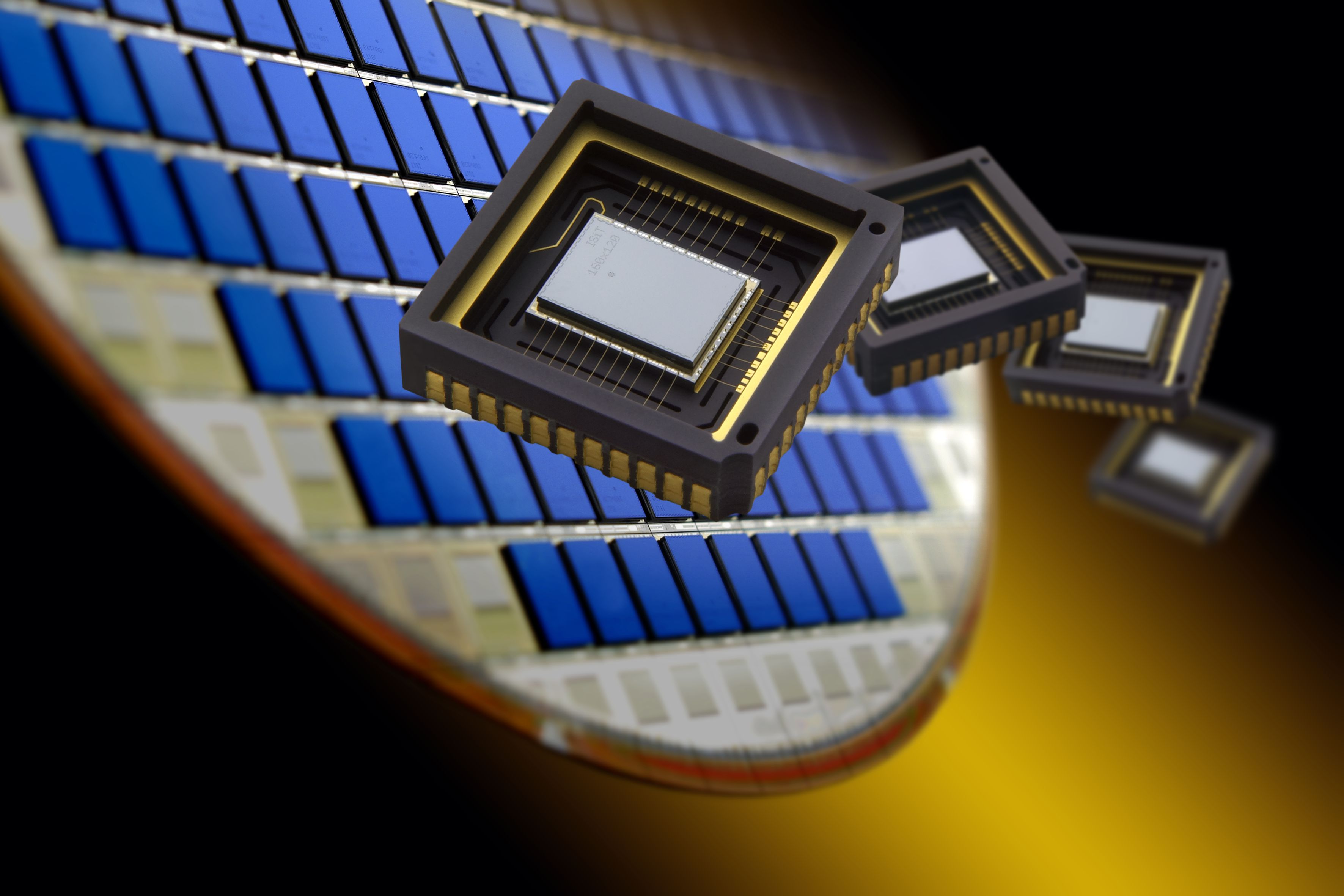
The housing of micro devices on wafer level exploits the high precision of semiconductor and MEMS processes to realize robust and very compact assemblies. ISIT focuses on hermetic (vacuum) encapsulation of micro sensors, actuators and micro optical components based on a number of different eutectic metal seal bonding technologies and glass frit bonding all with integrated getter. (Exponat: IR-Imager Wafer with IR-windows made if Silicon). For micro optical components, capping solutions with high optical transmission are available from the visual up to the far infra red range.
Wafer Level Packaging is suited also for post-CMOS processing of customer wafers. Application areas span from IR sensors and IR imagers to inertial and magnetic field sensors to harvesters and MOEMS devices.
The availabe infrastructure at ISIT is a modern 200 mm development line for microsystem components, glass-silicon compound substrate wafers with hermetic vias and functionalized cap wafers. The industrially oriented clean room is operated by a digital process monitoring system to enable a simple process transfer to volume manufacturing. Together with the in-house expertise in electrical testing, quality and reliability assessment and mass reflow technology ISIT can offer qualified packaged devices and assembled modules in a pilot production.
Opto-Packages for MOEMS and MOEMS Manufacturing
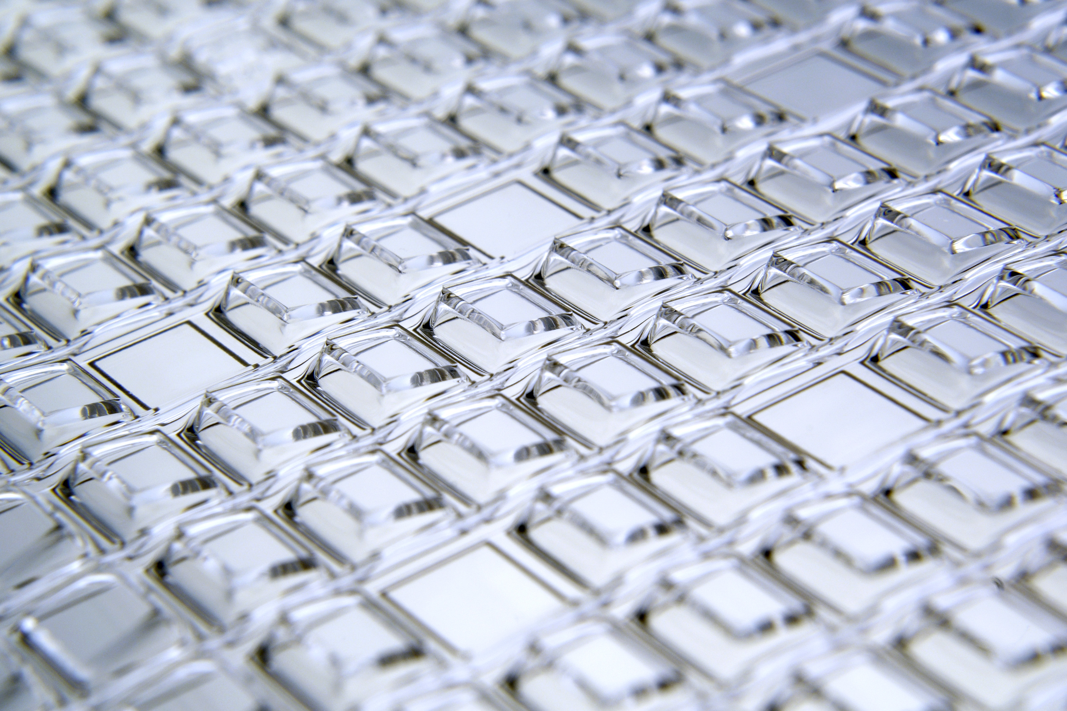
The development of structured glass cap wafers enables applications with special optical functionalities. The patented glass transformation technology platform with CTE matching to Silicon realizes micro lenses, reflectors and optical windows of specific geometries in large numbers on 200 mm wafer level without additional mechanical machining. The processing of micro optical elements is therefor very economic in high volume (Wafer with gold plated concave mirror). The glass forming platform is a key technology for the hermetic packaging of MEMS scanners and active optical devices that conform to high demands in respect optical functionalities (Exponat: MEMS mirrow with inclinded windows). The inclined windows prevent the back-reflection of the incoming laser beam into the projected picture. Packaged devices typically become part of larger optical systems and find applications in the areas of picture projection, structured light, optical data communication and material processing.
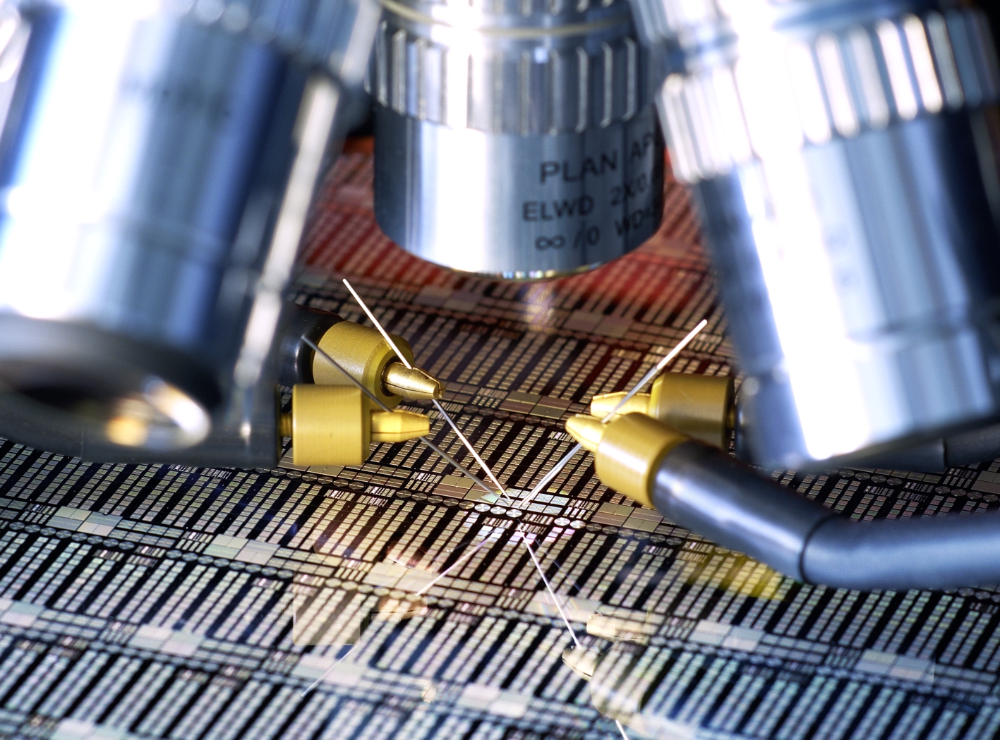
Quality and Reliability of Electronic Assemblies
The components of an electronic assembly are subjected to significant loads in connection processes, assembly and in field operation. Material, design and process control are the key factors in producing high quality products. Based on many years of experience analyzing of specific claims and accelerated aged pre-series samples, ISIT has generated a full range of development and service offerings that enable customers to actively increase the quality and reliability of their products.
The Productronica starts on Tuesday, November 12, 2019 and ends on Friday, November 15, 2019.
We look forward to your visit.