 Fraunhofer Institute for Silicon Technology
Press release | Outstanding development work
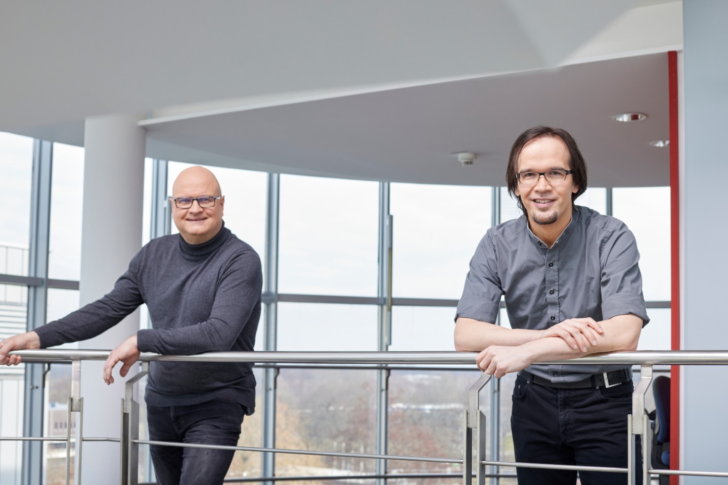
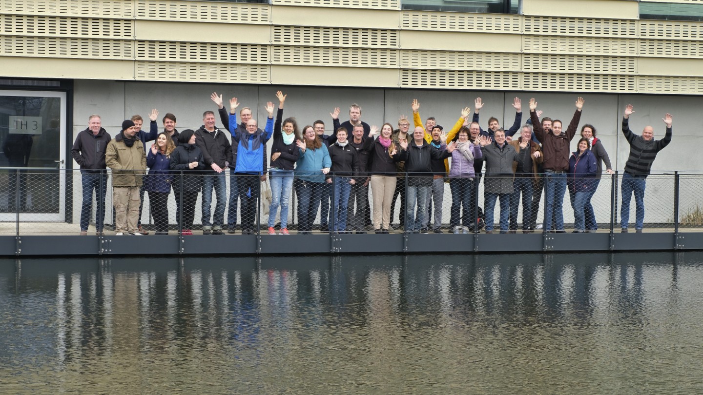
Fraunhofer Award 2021 for ISIT scientists Martin Witt, Michael Kampmann and Dr. Jacqueline Atanelov, IMS nanofabrication
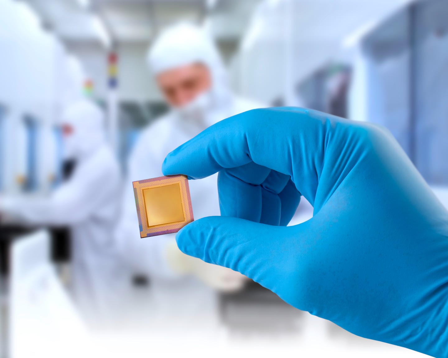
Since 1978, the Fraunhofer-Gesellschaft annually awards the prize for outstanding scientific achievements of its employees. This year, the jury awarded the two ISIT scientists Martin Witt and Michael Kampmann together with their colleague from IMS Nanofabrication. The President of the Fraunhofer-Gesellschaft Prof. Reimund Neugebauer presented the award yesterday in a festive setting at the Fraunhofer Annual Conference. The award was given for the processing of a microsystem switching element, which is the heart of an electron beam mask recorder. With their development, the scientists were able to push the previously reached limit a good deal on the way to ever smaller and more powerful microchips.

Smaller, faster, more powerful - that about sums up the constant development of smartphones and other electronic devices. At the heart of these devices are microchips, which also have to get smaller and better as part of this development. This has worked well for decades, but now a number of current manufacturing technologies are pushing structures to their limits.
World's only way
The only way out of this dilemma worldwide so far is offered by a novel technology: the electron multibeam mask recorder, developed by the Vienna-based IMS Nanofabrication GmbH. The key component for this device comes from Fraunhofer ISIT. "Whereas structures of just under ten nanometers in size could previously only be realized on chips - an atom is 0.1 nanometers in size - the new manufacturing process brings structures of seven nanometers and less into the realm of the feasible," says Martin Witt of Fraunhofer ISIT. This is unrivaled in a global comparison; for further miniaturization of chips, there is no way around the electron multibeam mask writer.
The fact that "IMS Nanofabrication GmbH was able to achieve its market-leading position with this technology" was also praised by the jury of the Josef von Fraunhofer Prize 2021 - and honored Michael Kampmann and Martin Witt from Fraunhofer ISIT as well as Dr. Jacqueline Atanelov from IMS GmbH with this award.

Privacy warning
With the click on the play button an external video from www.youtube.com is loaded and started. Your data is possible transferred and stored to third party. Do not start the video if you disagree. Find more about the youtube privacy statement under the following link: https://policies.google.com/privacyAward winning film microchips for the production of semiconductors
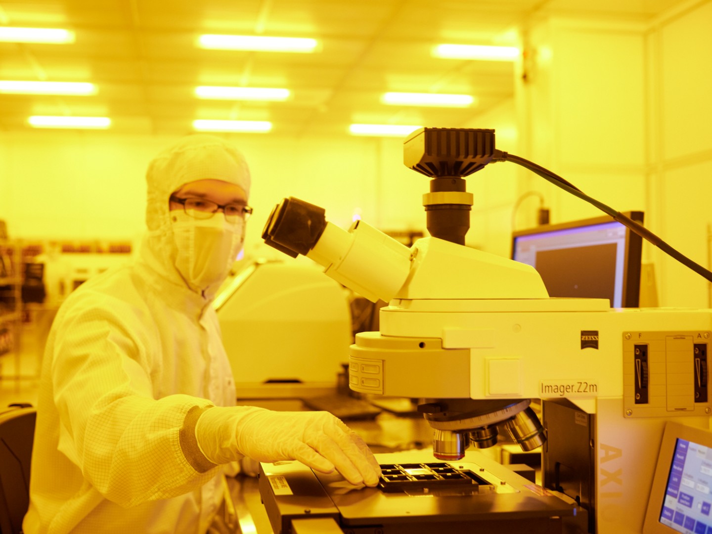
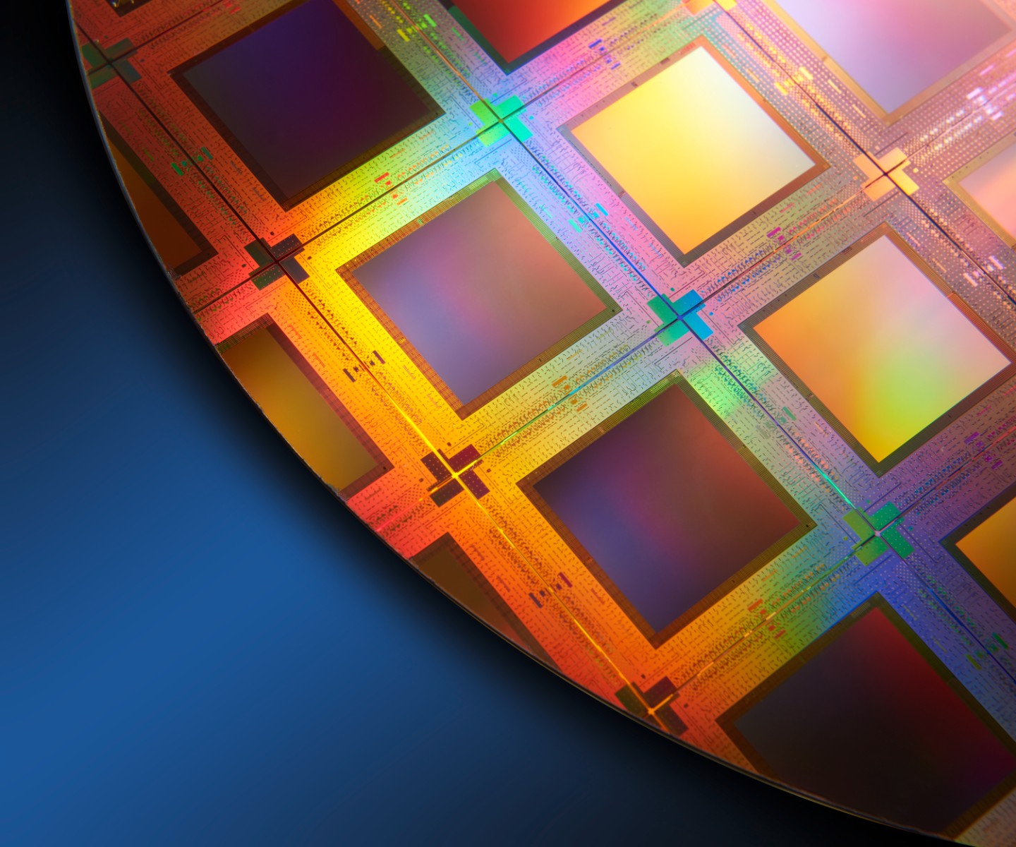
In order to be able to understand the prize-worthy development, it is first necessary to take a trip into conventional chip production. In this process, a wafer of the semiconductor material silicon is evenly covered with photoresist, which is selectively cured via light, the uncured areas are removed and the silicon is processed in the exposed areas. The cured part of the photoresist is then also removed and the process starts again from the beginning. In this way, the chip is created layer by layer - complicated chips require up to 70 exposure steps. Various masks are used to direct the light specifically to the areas where the photoresist is to be cured and to leave the other areas in the dark. These are manufactured in a similar way to the chips, but here an electron beam is used to cure the photoresist.
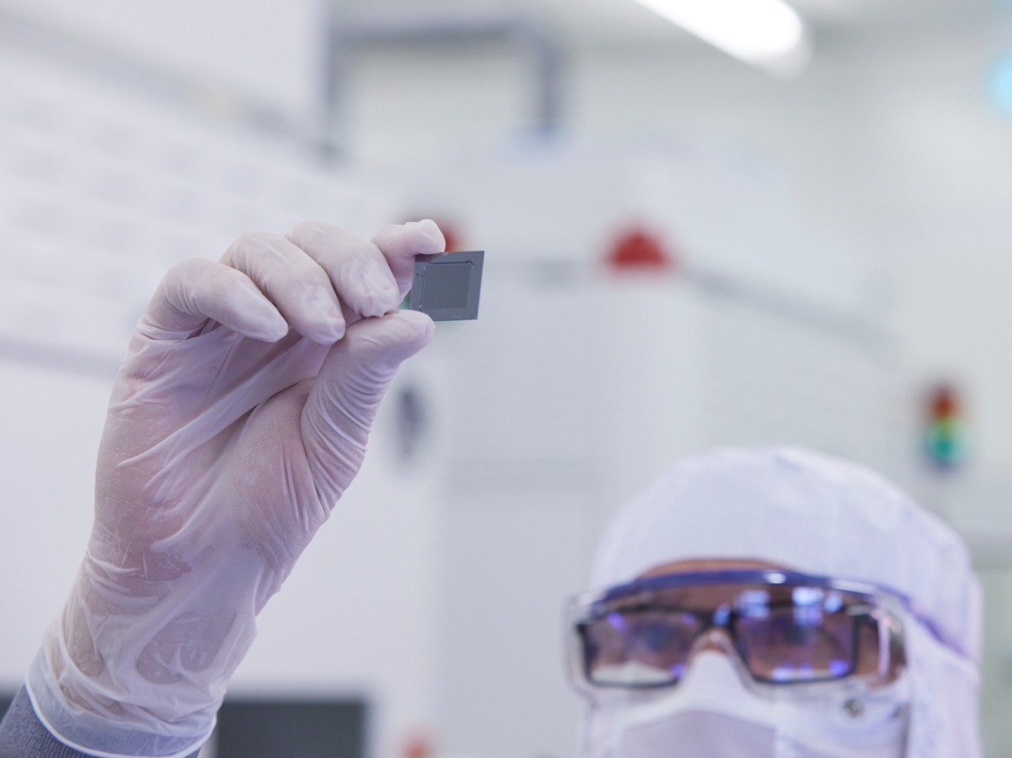
The highlight of the new process: "Instead of writing the mask structures on the electron-sensitive coating with a single beam, we use 512 times 512 beams, i.e. 262,000 beams," explains Kampmann. This is made possible by a Micro-Electro-Mechanical-System MEMS switching element from Fraunhofer ISIT - which forms the heart of the new multi-beam mask writer, so to speak. Put simply, this microsystem switching element resembles a membrane with 262,000 openings through which the electron beams can pass. However, these do not run parallel like water jets from a shower head, but can be individually controlled and deflected via special control electrodes.
Out of competition
"With the electron multibeam mask recorder, we can generate complex structures in high quality and resolution within a few hours," adds Atanelov. This makes the novel electron multibeam mask recorder unrivaled to date. Market demand is correspondingly high. IMS currently generates annual sales of 400 million US dollars with its devices. This is also noticeable at Fraunhofer ISIT: Industry sales significantly exceed one million euros per year. The award-winning technology thus not only enables further miniaturization, but also goes hand in hand with outstanding economic success.
Privacy warning
With the click on the play button an external video from www.youtube.com is loaded and started. Your data is possible transferred and stored to third party. Do not start the video if you disagree. Find more about the youtube privacy statement under the following link: https://policies.google.com/privacyMaking-Of Film about the winners of the Josef von Fraunhofer Prize 2021
.jpg)
.jpg)
.jpg)
.jpg)
.jpg)
.jpg)
.jpg)
.jpg)
.jpg)

.jpg)
.jpg)
.jpg)
.jpg)
.jpg)
.jpg)
.jpg)
.jpg)
.jpg)
.jpg)
.JPG)
.jpg)
.JPG)
.jpg)
.jpg)
.jpg)
.jpg)
.jpg)

.jpg)
.jpg)
.jpg)
.jpg)
.jpg)
.jpg)
.jpg)
.jpg)
.jpg)
.jpg)
.jpg)
.jpg)
.jpg)