 Fraunhofer Institute for Silicon Technology
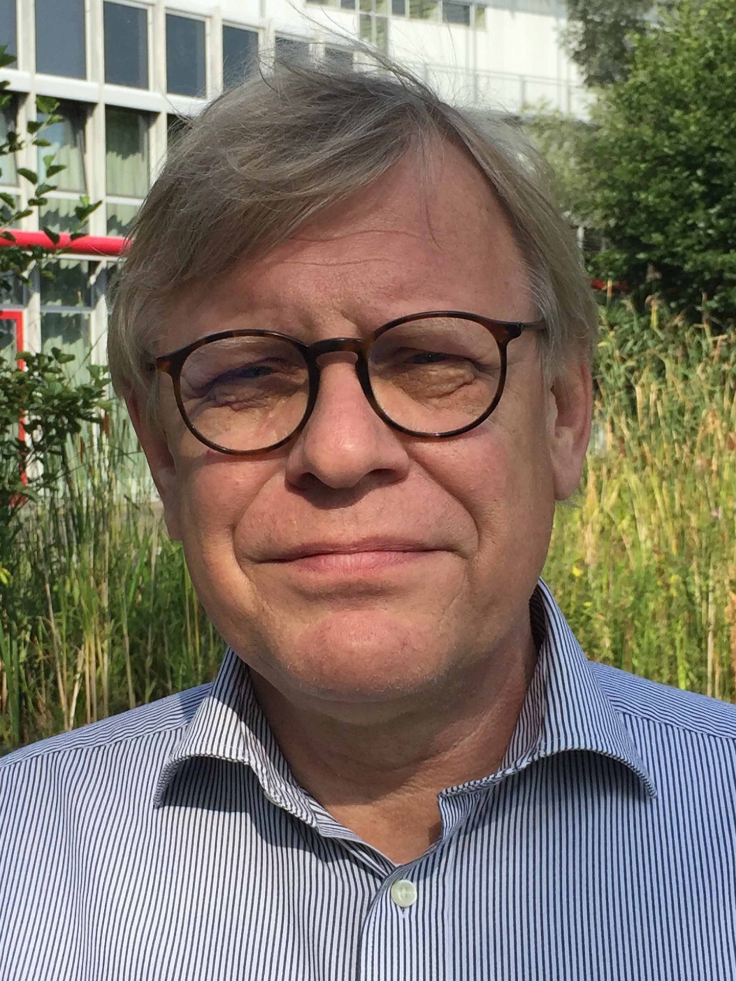
Fraunhofer ISIT scientist Dr. Gerfried Zwicker manages the meeting of leading experts in CMP within the scope of the International Conference on Planarization/CMP Technology ICPT 2017 on October 11 – 13 in Leuven, Belgium
Over the last 30 years chemical-mechanical polishing (CMP) has advanced from a simple method to planarize dielectric layers to a key enabling technology for the fabrication of microelectronic devices. Beside a procedure to reduce topography on the chip surface, which is needed to handle the very tight depth-of-focus requirements of advanced lithography techniques, CMP is employed for the structuring of the large number of copper metallization layers of integrated circuits (ICs), for the fabrication of dummy layers and structures for FinFET transistors or for the manufacturing of ultra-smooth surfaces of substrates for LEDs or GaN-based power transistors. Most advanced micro processors in 14 nm technology undergo up to 30 polishing steps in their production cycle.
Enough topics, to bring together CMP experts from all over the world to discuss latest developments and future applications. Therefore, the annual “International Conference on Planarization/CMP Technology ICPT 2017” has been organized by Fraunhofer ISIT scientist Dr. Gerfried Zwicker as conference chair together with VDE/GMM on October 11 – 13 in Leuven, Belgium, home of IMEC, the worldwide leading research institute for the advancement of microelectronics. 275 scientists, engineers, technicians and students from Asia, Europe and the USA followed the invitation and presented more than 100 oral talks and posters to the subject of CMP. Conference chair was Gerfried Zwicker from Fraunhofer ISIT.
The congress took place in the venerable halls of the Catholic University of Leuven and was connected with a small exhibition, where companies from the equipment and materials sector presented their products and additional information to the attendees.
A view beyond one’s own nose was given by two keynotes. Franz Laermer (Bosch corporate research), the inventor of the so-called Bosch process for the deep structuring of silicon, informed about the development and employment of microsensors from Bosch , which are applied million fold in cars and smartphones to save lives in traffic and to improve orientation in daily life. During the manufacturing of these microsensors, CMP is used for the smoothening of the rough poly-Si functional layers. Kathy Barla from IMEC discussed future technologies for most advanced devices, took a view on 3-dimensional scaling, and presented new materials for microchip fabrication. Finally, she showed that below structural dimensions of 5 or 3.5 nm, a performance improvement can only be achieved with system architectures beyond the classical von-Neumann architecture.
On this high-level conference, many very interesting presentations had been given and many very illustrative posters had been shown, which cannot be covered here in detail. Rather, some examples should highlight actual questions and problems, which have been discussed during the three days.
The fact that details of the removal process are still not yet fully understood has been discussed in the CMP Fundamentals session. Ara Philipossian from the University of Arizona in Tucson reported on new methods for the determination of the thickness of the slurry film between polishing pad and the substrate to be polished. For the damascene metallization layers at the Back End of Line (BEOL), beside Copper the old standard metal Aluminum and recently Cobalt and Nickel are now under consideration. Developments of novel slurries for these materials have been presented. Furthermore it has been reported that certain Ceria-based slurries, against normal expectations, are showing increased removal rates with higher dilution with water until up to about 7 : 1, which can be explained by an increase of the removal-rate determining concentration of Ce3+ in the dilution.
Insufficient removal of particles from the polishing slurry leads to defects and thus a reduction of yield. Scientists from the CMP tool manufacturer Ebara and the University of Yamanashi, Japan, presented very interesting investigations on the measurement of the number of particles using ellipsometry, a measurement technique abundantly available in fabs, and on the determination of the force needed to remove particles, using atomic force microscopy (AFM). Both investigations will help to improve the understanding of post-CMP cleaning processes.
Process control plays a very important part when employing CMP in chip manufacturing. Cedric Perrot from CEA/Leti (France) showed that a much more conscientious view on friction mechanisms can lead to much more precise endpoint signals to control and stop the polishing process. At today’s technology nodes, nanotopography, i.e. very minute variations in the range of 10 nm in the flatness of the surfaces to be polished show a great influence on film thickness variations after polishing and has to be considered specifically, as investigations at CEA/Leti and IMEC have turned out.
Moore’s law, which has described the increase in integration density of ICs very precisely over the last 50 years, is running out of steam. Therefore, all technologies for chip manufacturing have to be examined and new paths have to be followed, including CMP. So, in a witty invited talk, Manabu Tsujimura from Ebara called for Innovation! Innovation! Innovation! and showed with a few examples, that CMP further on can play a key role in advanced chip manufacturing, when employing existing technologies innovatively.
Beside the presentation of three Best Student Paper Awards for outstanding talks and posters to junior scientists, Suryadevara Babu from Clarkson University (USA), Jin-Goo Park from Hanyang University (Korea) and Gerfried Zwicker from Fraunhofer Institute for Silicon technology (Germany) have been honored in a short ceremony with the “Lifetime Achievement Award for Distinguished Contributions to the Field of Planarization” for their dedication to the advancement of chemical-mechanical planarization CMP.
The highlight of the conference was a banquet dinner in the medieval buildings of Leuven’s Great Begijnhof, which is part of the UNESCO World Heritage since 1998. Especially the conference attendees from Asia and the USA were impressed by the well-restored Begijnhof and the medieval character of the City of Leuven in general. The three conference days were perfected by a windows tour offered by IMEC (Interuniversity Microelectronics Centre), an opportunity thankfully taken by many of the highly interested participants of ICPT 2017.