 Fraunhofer Institute for Silicon Technology
Jan Lähn
Challenges in the assembly of smallest components in the SMD process
Within the framework of various development projects, Fraunhofer ISIT has developed guidelines for the safe processing of miniaturized components for a component manufacturer.
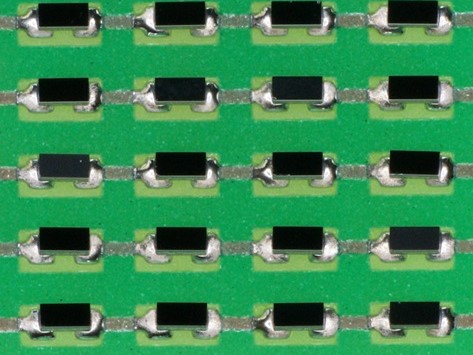
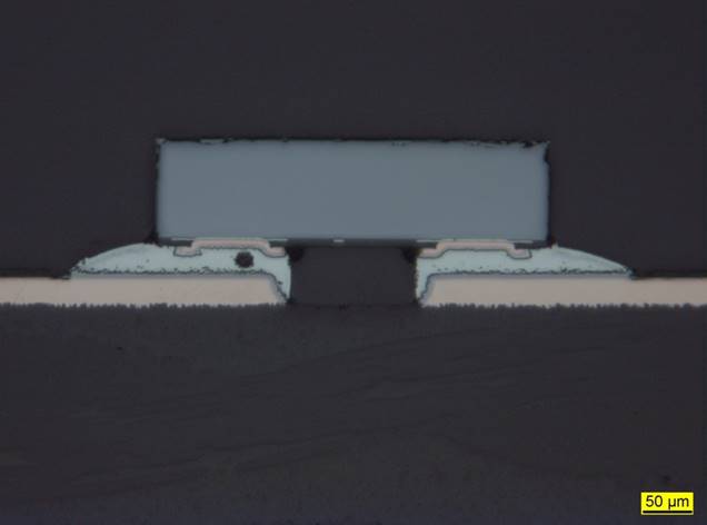
A component with dimensions of 0.4 mm x 0.2 mm edge length with solder terminals (DSN0402) on the underside must be able to be processed safely in an SMT manufacturing process. Together with significantly larger components (coils, ICs, connectors), very high demands are placed on the manufacturing and delivery quality of the PCB supplier and the solder paste.
There are some things to consider, read our TechBlog.
printed circuit board
The pad layout must be specially adapted to avoid tilting of the components during the soldering process as far as possible. There is a high demand for lowest manufacturing tolerances, especially for the solder resist and pad surfaces (undercutting). The connection of the pads also plays a role. It makes a clear difference whether the connections are made via a microvia (which should be plugged) or via a lateral connection covered by solder resist.
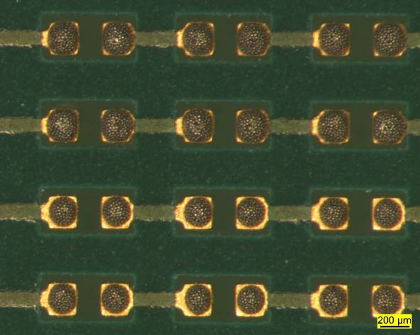
Solder paste printing stencil
The opening sizes should always be calculated exactly in relation to the stencil thickness, the area ratio (AR) plays a very important role here. Rounded edges in the apertures, as well as a non-stick coating, have a significant influence on the release behavior of the printed solder paste. For mixed assembly with larger components a stepped stencil may have to be considered.
Solder Paste
By default, a solder paste with a fine grain size must be selected for processing the smallest components. To achieve sufficient volume in the solder joint, a solder paste of class 4 or 5 is usually used here.
Mounting/soldering process
SMD components are set up in so-called reels on an automatic placement machine. Particularly fine vacuum nozzles in the placer as well as very precise feeder feeds are necessary to safely remove these smallest components from the tape. There are also special requirements for antistatic properties.
The soldering process is usually carried out in a multi-zone convection reflow oven under inert gas atmosphere (<500ppm residual oxygen) or in a condensation soldering system (vapour phase).
Summary
With its technological know-how, ISIT offers a wide range of services from design development to the finished product and the corresponding analysis options. Layouts for miniaturized components are developed in cooperation with suppliers of printed circuit boards, stencils and machines. We are happy to assist you with the introduction of new technologies, you can contact us at e.g. Mail.
This might also be of interest to you