 Fraunhofer Institute for Silicon Technology
Jenik Grimsmann
Cycle time reduction in the SMD manufacturing process using the example of a customer assembly by optimizing a convection soldering process while preserving quality.
At Fraunhofer ISIT, the working group Module Services of the business unit Micro-Manufacturing Processes realized the cycle time reduction on a convection soldering oven while maintaining quality as part of a final thesis for the training of a microtechnologist.
The starting point was an existing soldering profile. This was to be optimized in such a way that an increase in throughput could be achieved without any loss of quality in the finished product.
To this end, simulation software was first used to develop a proposal for a furnace setting by varying the transport speed and the temperature of the individual heating zones as parameters.
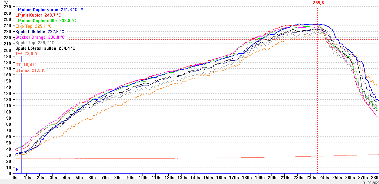
Temperature measurements were then carried out on a sample assembly. For this purpose, type K sheath thermocouples were applied to solder joints and to thermally sensitive components. The objective in the soldering process was to provide sufficient heat at the solder joints for a substance-to-substance solder joint without overloading heat-sensitive components or the printed circuit board. The result of the measurements were three potential parameter sets for the furnace setting. The pattern of a temperature measurement curve is shown in Fig. 1.
Analysis of the temperature measurements showed that as the transport speed increased, both the solder joint temperatures and the times above liquidus (solder in the molten phase) decreased.
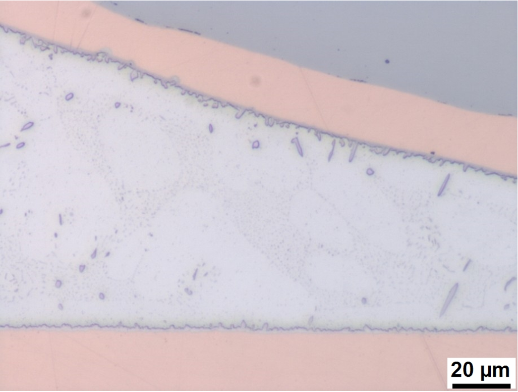
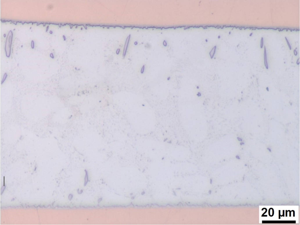
With the sets of parameters developed, test samples were built and a quality check was performed on the assembly samples. Both visually and by X-ray inspection, no significant differences were seen between the different solder profiles. All assemblies showed no solder defects, damage or abnormalities. A cross-section analysis followed to assess both solder joint quality and structural integrity of the assembly. Damage to components or PCB could not be detected even in the cross-section. All solder joints exhibited good wetting and a continuous intermetallic phase layer. Only the solder profile with the highest transport speed showed a slightly reduced intermetallic zone, see Figs. 2 - 3.
In the production process of electronic assemblies, there can always be fluctuations in the quality of the materials supplied. For example, the thickness of the supplied printed circuit boards can vary by +/- 10% and still be within the permissible process window. However, this tolerance has a decisive influence on the heat capacity of the assembly. Borderline cold soldering profiles could lead to non-soldering in the case of a thicker PCB (higher soldering heat requirement).
In order to make the soldering process more stable and less susceptible despite increased throughput, i.e. to widen the process window of the soldering process, not the tested maximum transport speed was selected for parameter optimization, but a somewhat slower speed. In this way, a significant increase in throughput was achieved while maintaining quality, thus achieving the goal of the project work.
ISIT offers technology consulting and support for process evaluation and optimization. We are at your disposal for individual questions.
This might also interest you