 Fraunhofer Institute for Silicon Technology
Tim Alexander Barnbrock
Safe current measurement in SIR tests at high voltages
For the qualification of materials used in electronics manufacturing, such as flux and solder resist, measurements of the surface insulation resistance are carried out at ISIT, among other things. For this purpose, e.g. flux or solder paste is applied to test structures, subjected to a soldering heat load and then aged under applied DC voltage in a test climate.
The increasing prevalence of high-voltage applications in power electronics and in the automotive sector requires the performance of such SIR test measurements (SIR = Surface-Insulation-Resistance) under high voltages. The development of a test stand for up to 1,500 V applied voltage was implemented as part of a bachelor thesis.
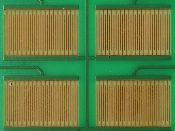
In SIR tests, the test objects are exposed to climatic stress in order to simulate operation of the electronic assemblies in a demanding environment over a longer period of time. Due to the prevailing temperatures and high humidity, aging phenomena occur at an accelerated rate. In this way, the test period can be significantly shortened compared to operation under real conditions, typically to one to several weeks. During this climatic aging, electrically conductive structures known as dendrites can grow as a result of ECM (electrochemical migration). As a result, the surface insulation resistance continuously decreases and can ultimately lead to short circuits when bridging conductors of different potentials. To test this development; test structures can be integrated into a functional layout or, as in Figure 1, consist of an exposed comb structure whose combs do not touch each other. There is no solder resist between them, so a reduction in surface insulation resistance is most likely to occur there.
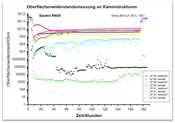
Figure 2 shows a typical course of the measured values during a one-week SIR test. The climatic conditions corresponded to the standard parameters of 85° C and 85% relative humidity. The components investigated were resistor arrays of type RN58. Exposed comb structures as well as comb structures under RN58 were investigated.
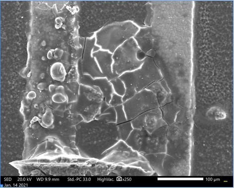
The scanning electron micrograph from Figure 3 shows at 250x magnification the environment of one of the components, which are represented in the green graph from Figure 2. The permissible limit of 100 MOhm (1E8 ohm) was significantly undercut, which can be explained by the grown dendrites. The resistance did not drop to near zero because there are protective resistors in the measurement circuit to limit the current.
Another method of qualification is H3TRB (high-temperature-high-humidity reverse bias) tests. These take place under comparable climatic conditions, but are specifically used to qualify semiconductor transistors. A voltage is applied between the drain and source terminals. The base voltage, which is also present, is below the threshold voltage of the transistor, which thus does not conduct in the initial state of the test. Due to the high climatic stresses, the properties of the semiconductor may be impaired. A breakdown of the base voltage can be the result. Unlike SIR tests, this method records and evaluates the leakage current, rather than the resistance.
As part of the bachelor's thesis, an 80-channel measurement system was developed in which a different voltage can be assigned to each channel. This is suitable for both test methods. Thus, materials and semiconductor devices from the high voltage range can be tested at ISIT in the future.
Please do not hesitate to contact us with your requirements.