 Fraunhofer Institute for Silicon Technology
Artem Kormann
Solder paste qualification of low-temperature SnAgBiXx solder pastes based on selected solder paste tests
Due to cost pressure and for reasons of climate technology, packaging technology is faced with the task of making manufacturing processes more cost-effective as well as more energy-saving and thus more climate-friendly. One answer to this challenge is the development and use of low-temperature solders, which can already be used in many areas such as the production of white goods (household appliances), consumer electronics, lighting with LED technology and many other applications. Due to the low ambient and operating temperatures of these electronic assemblies and systems, a low melting point solder alloy is suitable for manufacturing.
Bismuth-containing low-temperature brazing alloys offer a number of advantages here:
- significantly lower energy consumption in the reflow soldering process due to the lower reflow peak temperatures compared to the standard SAC soldering process (approx. 250°C in the SAC soldering process → approx. 180-200°C in the low-temperature SnBiX soldering process),
- lower warping (bending) of the composite partners due to lower thermal expansion in the soldering process,
- lower thermal stress on the assemblies in the manufacturing process.
As part of a reliability investigation of electronic components soldered with SnBiX solder, a microtechnologist's final thesis was conducted on the topic of "Solder paste qualification of low-temperature SnAgBiXx solder pastes based on selected solder paste tests".
The qualification was performed on three solder pastes (paste A, B, C) with similar alloy. The solder pastes have the following characteristics:
- Alloy: SnBiXx (tin-bismuth-Xx),
- Standard powder size type 4 according to J-STD-005 (type 4: 20-38µm ball diameter),
- Melting range approx. 138°C-140°C.
For solder paste qualification at Fraunhofer ISIT, tests are used that cover all essential manufacturing processes of electronic assemblies. Thus, a solder paste has to be evaluated in solder paste printing, component placement and the soldering process:
Solder paste printing:
- Release behavior from the SMD stencil
- Contour stability of solder paste deposits (slump test)
Placement process:
- Tackiness of the solder pastes (Tackiness Test)
Soldering process:
- Wetting properties of solder pastes (Solder Spreading, Wetting Test)
- Melting behavior (Solder Ball Test)
- Pore formation in the solder structure (Voiding Test)
- Surface insulation resistance (SIR test)
In the following, the solder spreading test and the slump test are explained in more detail.
Solder Spreading Test
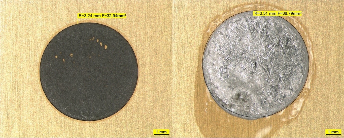
The solder spreading test is a test for analyzing the wettability of a solder paste. In this test, a round solder paste deposit is printed onto a wettable, metallized surface and then remelted.
Wetting is evaluated by comparing the wetted area after the soldering process with the area originally printed with solder paste. A comparison of the printed as well as subsequently wetted area on a NiAu metallization can be seen in Fig. 1. For the evaluation of the solder spreading test, the structures can be assigned to the following wetting categories after the comparison:
- Category 1: Wetting is greater than the printed area → Ideal / passed
- Category 2: Wetting is exactly as large as the printed area → Sufficient / passed
- Category 3: Wetting is only partial → Poor / failed
- Category 4: Wetting is smaller than the printed area → Poor / failed
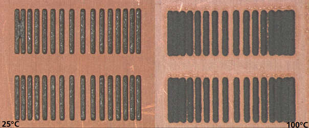
Slump Test
The slump test examines the contour stability of a solder paste after printing. Here, the horizontal and vertical "flowing away" of a solder paste is analyzed. The word "slump" stands for the collapse of the solder paste depot edges after solder paste printing, which can ultimately lead to the merging of adjacent solder paste depots and thus to the formation of short circuits in the soldering process. Particularly in fine-pitch applications, i.e. components with small pin spacing and consequently solder paste depots with minimal spacing, a paste with insufficient slump properties is not suitable because it does not ensure sufficient contour stability.
To perform the slump test, fully metallized areas of test PCBs are printed and then stored at defined conditions under different temperatures.

If you are interested in further information or if you want to analyze your solder paste printing process in more detail and e.g. compare different solder pastes, you are welcome to contact ISIT. Likewise, we carry out investigations for the selection of the suitable solder paste print stencil combination and work out layout recommendations for you in the form of "Application Notes".