 Fraunhofer Institute for Silicon Technology
Wolfgang Reinert und Alexander Barnbrock
Process testing for micro-optical systems - A multifunctional precision assembly system enables the construction of complex prototypes
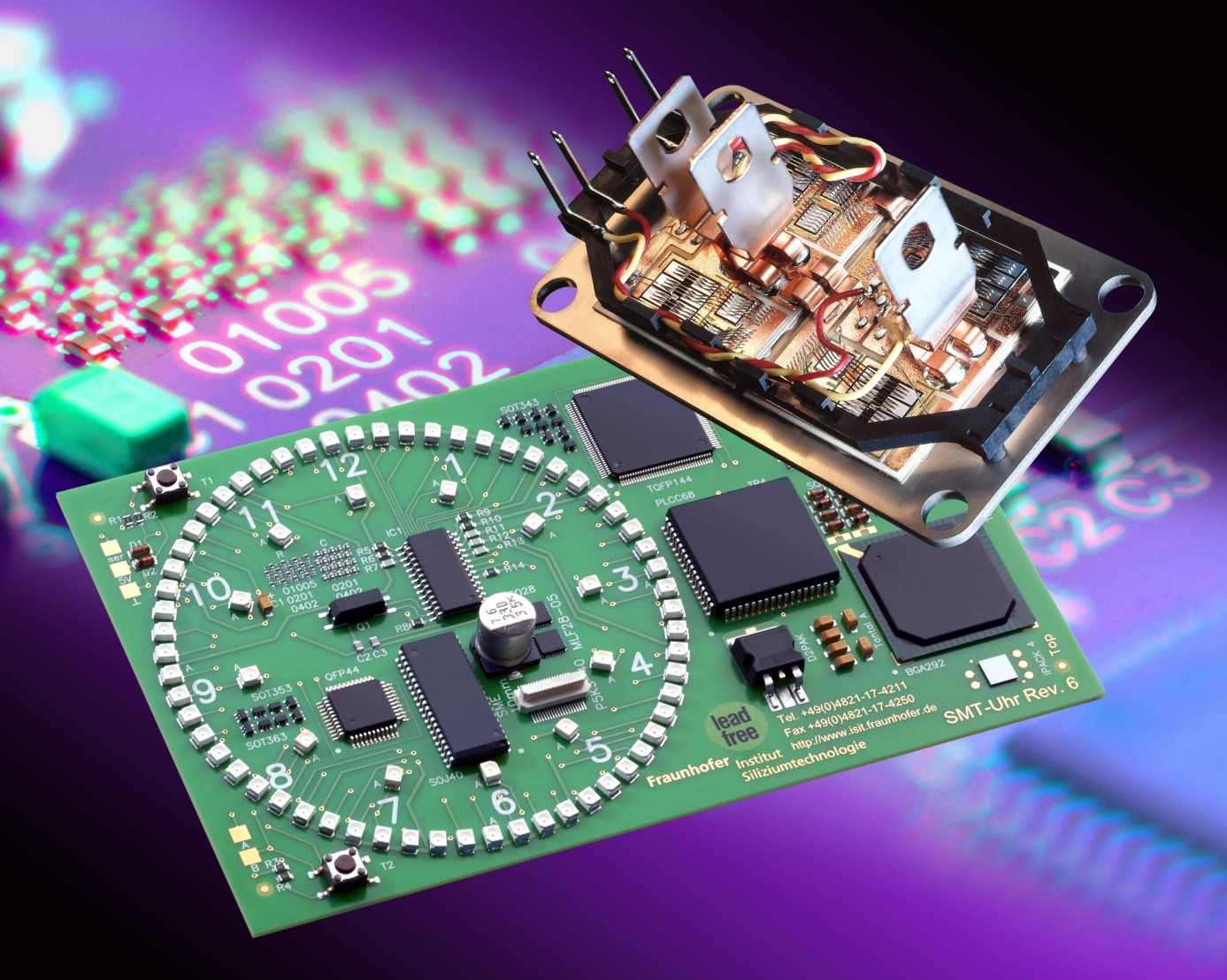
Producing functional samples or prototypes of miniaturized electro-optical systems can be a major challenge, especially for small companies. The implementation of innovative ideas is often accompanied by the need for suitable machines with which the new manufacturing steps can be realized. The acquisition of such special equipment for experimental purposes represents a financial risk. An addition to the process capacities of Fraunhofer ISIT's Assembly and Joining Technology (AVT) helps to mitigate this risk.
For some time now, ISIT has had a high-precision assembly system from the company FiconTec, whose capabilities in the areas of component handling and joining techniques allow for a wide range of applications.
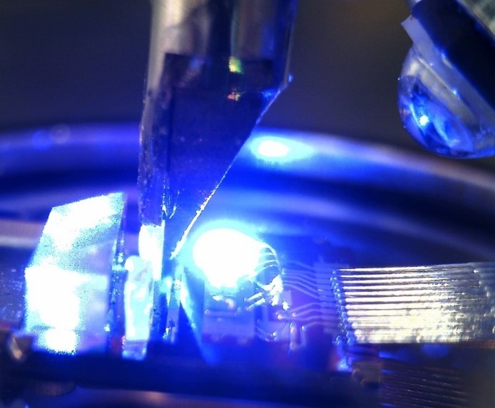
This system, which is divided into two modules, allows microcomponents to be assembled with an accuracy of up to 0.6 µm. This precision is made possible by freely programmable image recognition and piezo motors. Unhoused laser diodes can be operated during the process to, among other things, precisely position collimating lenses in the beam path of the laser diodes (see Figure 1).
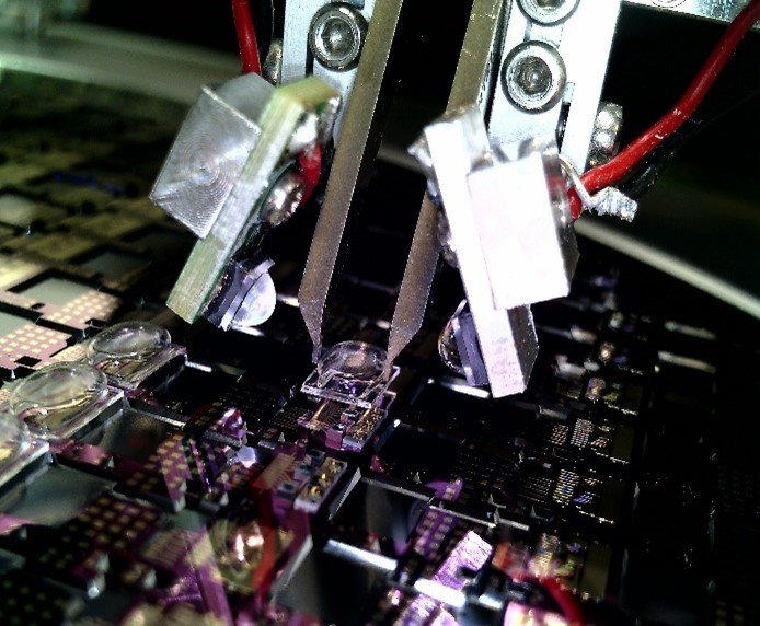
32 freely programmable axes and a variety of tools are available. These include suction cups and grippers (see Figure 2), and application-specific tools and carriers can also be implemented. An integrated touchdown sensor and a flipper allow components to be precisely picked, positioned and held during attachment in all angular positions. This is done either by means of a solder laser or by applying and irradiating UV-curing adhesive. Both variants can be carried out in-situ, since the corresponding devices are installed in the system and can be operated simultaneously with the positioning tool. A noteworthy feature of the laser is its ability to act on the solder joints through a substrate (silicon or glass) and thus solder individual components in a minimally invasive manner. The substrate is hardly heated, as it is transparent to the wavelength of the laser beam.
In the meantime, the components are fed to the second module, which uses a robotic arm to remove the required parts either from gel or waffle packs, or from a wafer, and delivers them to the main module via a transport carriage. Application-specific tools can also be implemented for the second module.
Possible processes through a panel and/or wafer-based assembly concept
- Die-Bonding
- Flip-chip bonding
- Wire bonding (modules and also on wafer level up to 300 mm Ø)
o Thin wire (Wedge-Wedge (aluminum wire) or Au-Ball Wedge)
o Thick wire (Wedge-Wedge)
o Ribbon bonds - Hermetic wafer bonding
o with cap wafers with optical interface made of glass or silicon
(e.g. for infrared applications)
o with backfill (possible with various gases) in order to create a
defined atmosphere and to protect sensitive components (such
as laser diodes) from environmental influences.
- Soldering processes
o reflow soldering
o Vapor phase soldering
- Wafer-level metrology
- Separation
ISIT combines this multitude of processes with the possibilities of wafer fabrication in ISIT's own clean room and thus enables the fabrication of e.g. silicon wafers as optical integration platforms with conductive tracks, solder pads, recesses, bond frames and V-grooves.