 Fraunhofer Institute for Silicon Technology
Dry Etching and Ashing
Ashing process is used to remove the photoresist from an etched wafer using an oxygen plasma.
Reactive Ion Etch (RIE)
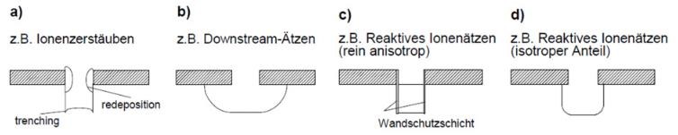
The reactive ion etching is an ion-assisted reactive etching process. Because of the good controllability of the etching behavior (homogeneity, etch rate, etch profile, selectivity), RIE is a method for the production of topographical structures for micro- and nanosystem technology. The process allows both chemical-physical removal of both an isotropic (direction independent) and an anisotropic etching. The etching is performed by charged particles (ions) generated in a gas plasma. A corresponding masking (eg generated by photolithography) of the surface gives the shaping of the structures. In reactive etching, the chemical etching reaction is triggered only by the kinetic energy of the incident ions. From the gas ion and the layer molecule of the surface, the volatile etching product is formed, which is removed by the vacuum system. RIE provides very good results even with very fine structures with dimensions well below 100 nm.
Characteristics:
Selectivity, etch profile, etch rate, homogeneity, reproducibility - is precisely adjustable in reactive ion etching by the gases used and the process parameters (generator power, pressure, gas flow). Both an isotropic and an anisotropic etch profile are possible.
Application areas:
- Semiconductor technology
- microreactors, micro flow sensors, microswitches, optocouplers, micromotors, biosensors
- Smallest components for movable and immovable microstructures
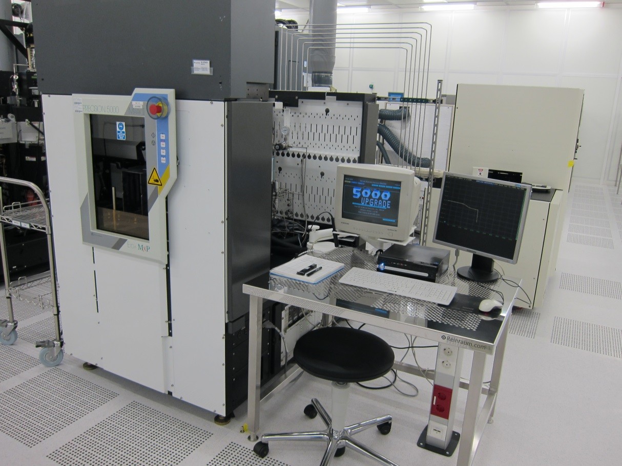
Equipments:
- Applied Materials
- Precision 5000 with MxP + chamber
- Single wafer process
- Endpoint detection: optical emission, laser interferometry
- Helium backside cooling
- Clamping by electrostatic chuck
Deep Reactive Ion Etch (DRIE)
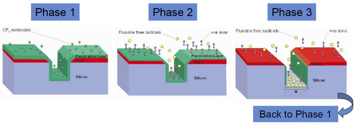
Reactive ion etching is a further development of reactive ion etching and was developed by Robert Bosch GmbH in the early 1990s. Reactive ion etching is a further development of reactive ion etching and was originally developed in the early 1990s by Robert Bosch GmbH. Therefore, the process is also called "Bosch process". It was further developed in the following years and made commercially available. This improved process is marketed together with the plant technology under the name "Advanced Silicon Etching" (ASE). The DRIE process is a highly anisotropic dry etching process for the production of silicon microstructures. The method is iterative and based on the use of a passivation layer which, in conjunction with a superimposed DC voltage, causes anisotropy in the etching process. The goal is to etch as anisotropically perpendicular to the substrate surface.
Characteristics:
Selectivity, anisotropy and etch rate are adjustable by gases and process parameters (RF power, pressure, gas flow, substrate cooling, etc.). Anisotropy is achieved by sidewall passivation.
Process-steps:
Step 1: Passivation with polymers (C4F8)
Step 2: Opening the polymer by directional particle bombardment (SF6)
Step 3: Isotropic etching of the silicon on the etching ground
Application areas:
- Sensor technology
- Actuator
- Micro-optics
- Microfluidics
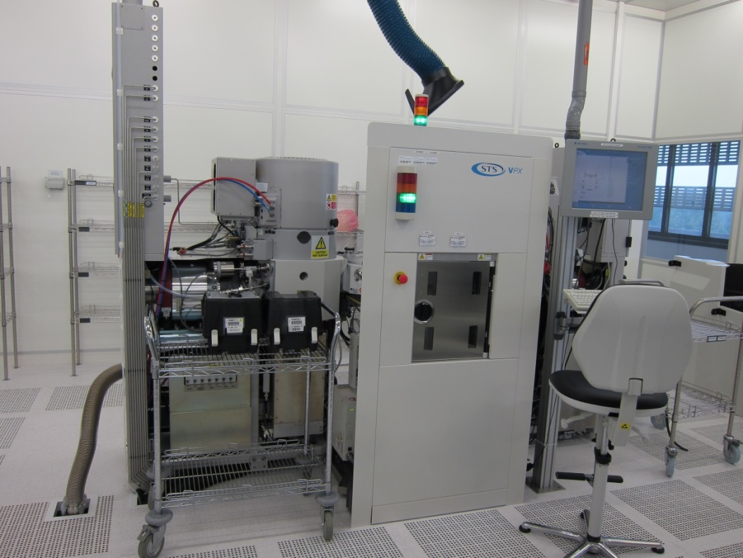
Equipments:
- SPTS Pegasus, high-rate etcher is operated on the ASE
- Only SF6 and C4F8 in process
- Connected gases: SF6, C4F8, O2, Ar
- RF coupling through a coil (ICP)
- Helium backside cooling
- Clamping by electrostatic chuck
- Edge protection possible
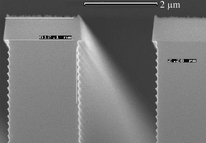
Performance Data
| Aspect ratio (Depth:Width) | up to 30:1 |
| Flank angle | 90° +/- 2° |
| Etchrate | up to 10µm |
| Maximum etching depth | Through wafer etch possible (725µm) |