 Fraunhofer Institute for Silicon Technology
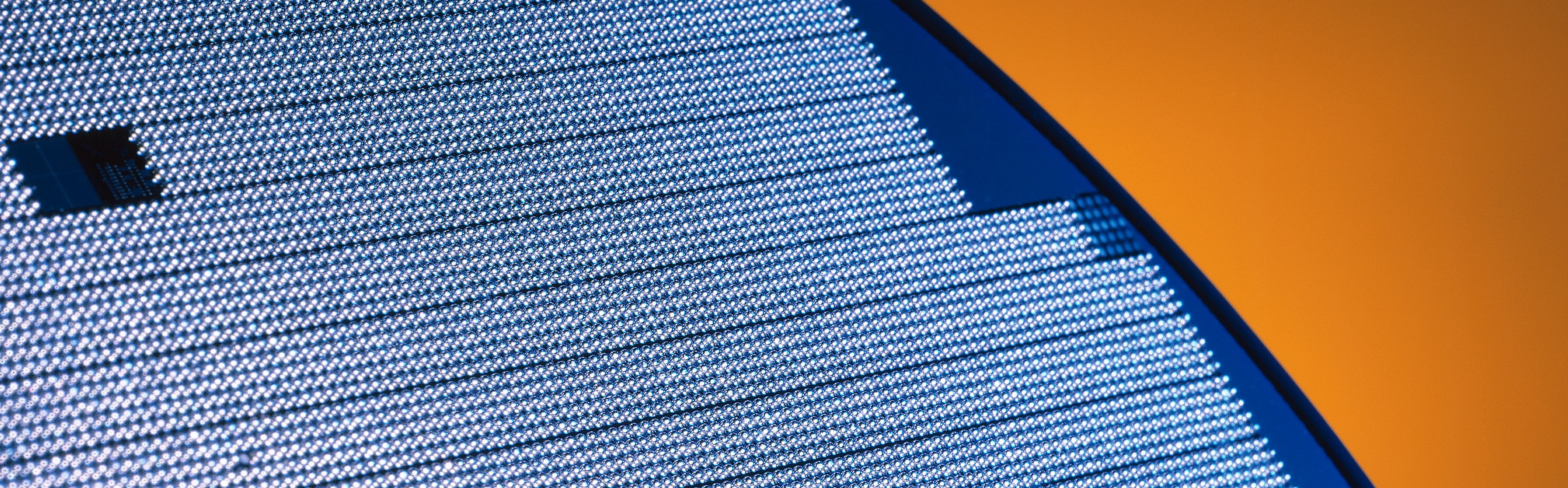
Solder balling of wafers and substrates can be done by two different technologies: Preformed discrete solder balls are usually applied to WL-CSP devices. The available infrastructure is able to handle wafers up to 300mm in diameter. If required, a solderable under bump metallization can be applied by electroless NiAu deposition. Solderballs with a diameter as small as 200µm can be placed in a pitch of 400µm with very high yield. The process has been proven to be reliable for TAIKOTM wafers with a remaining thickness of 30µm.
Smaller Pitches can be realized by solder paste printing which is reliable on an industrial scale down to a pitch of 250µm.
Characteristics:
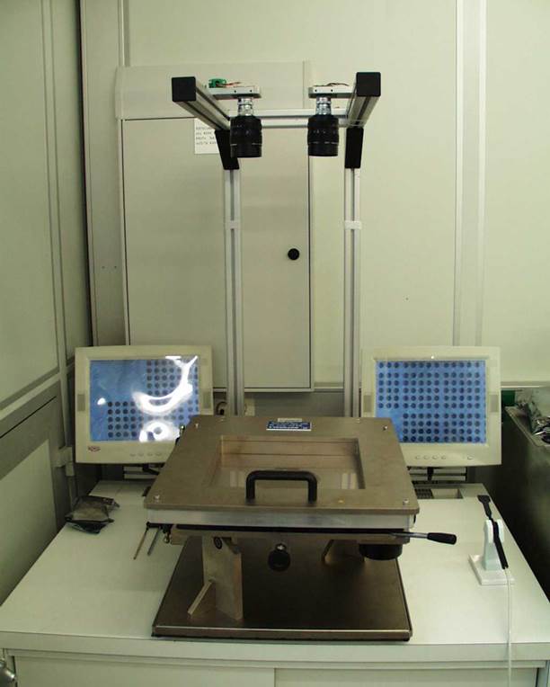
Placement of discrete solder balls or printed solder paste on thinned wafers with up to 300mm diameter.
Process Steps - Balling:
- Step 1: Flux printing
- Step 2: Placement of discrete solder balls
- Step 3: Soldering
- Step 4: Cleaning
Process Steps – Bumping:
- Step 1: Solder paste printing
- Step 2: Reflow
- Step 3: Cleaning
Applications:
- Wafer-level chip-size packaging (WL-CSP)
- Flip-chip