 Fraunhofer Institute for Silicon Technology
Mario Reiter
Development, production and provision of test wafers with structures in glass or silicon
Material screening, process development and machine qualification are typical scenarios for the use of test wafers. While product wafers are usually expensive and difficult to procure, test wafers can be produced cost-effectively and tailored to the respective requirements. In addition to standardized components for typical applications, ISIT also offers customized solutions.
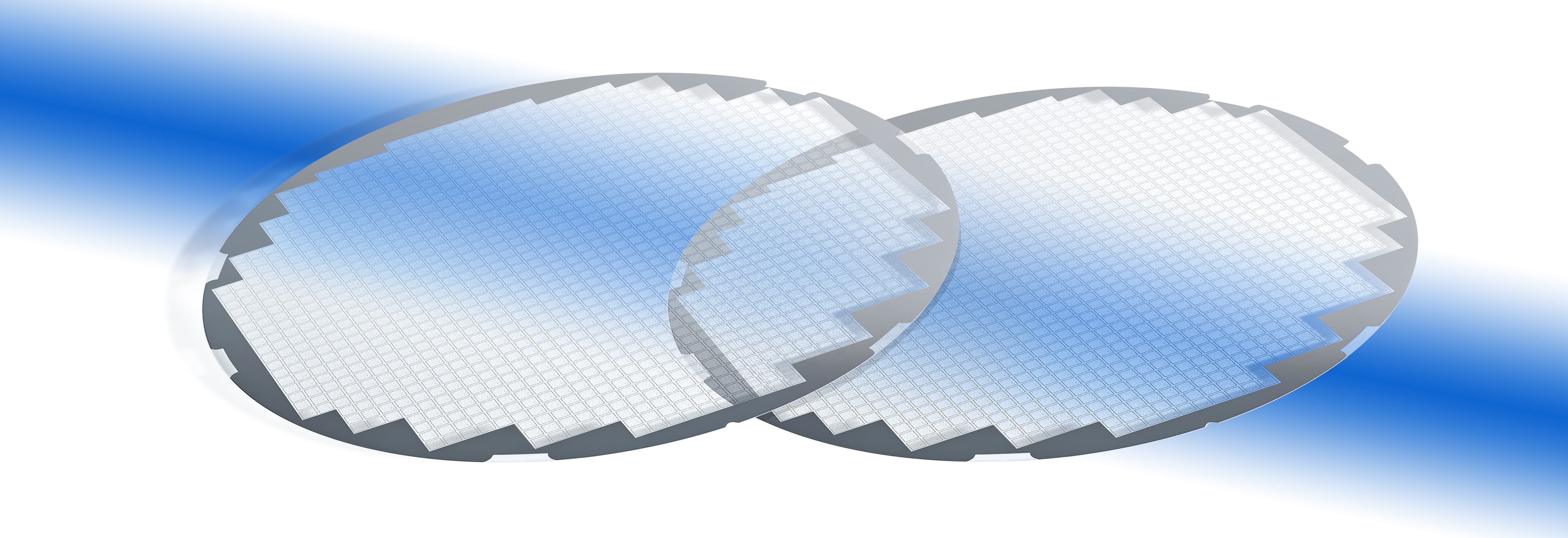

Different carrier materials (glass wafers, silicon wafers) are available. The wafers are manufactured in 8 inch format, i.e. the wafers are round and have a diameter of 200mm.
There are 2 surfaces (top / bottom of the wafer) available for treatment. The wafers can be coated with different metallic surfaces (e.g. Al, Cu, Ni, Au, Ag).
For different layer thickness ranges (nm- range to µm- range), correspondingly different metal deposition variants (e.g. evaporation, sputtering, galvanic metal deposition) are available. To guarantee the adhesion strength of the metals on the wafers, adhesion promoter layers are used. Various plating base systems (such as WTi, TiPtAu, CrAu) are used as adhesion promoter layers.
In addition to metal deposition, insulator layers (e.g. Si3N4, SiO2) can also be generated.
By using appropriately patterned exposure masks, the wafers can be patterned almost arbitrarily down to the submicrometer range. Depending on the accuracy requirements, the wafers are exposed completely or in partial steps (with so-called steppers). Several exposure or process levels are possible on one wafer. When creating the mask layout, ISIT employees, who have many years of experience in mask design, use common design tools. This is followed by the procurement of the physical masks.
The 8-inch silicon or glass wafers have a standard thickness of 725µm. Glass wafers can also be provided with lower thickness (e.g. 400µm). If required, the wafers can be thinned by a subsequent grinding process (silicon wafers to about 100µm, glass wafers to about 200µm).
Depending on the application (size), up to several 100 individual chips fit on an 8 inch wafer. To separate these, the wafer is laminated onto a foil and cut into the appropriate individual chips. Typical cutting widths for silicon wafers are 35µm. It is also possible to offer grinding and sawing processes as a service, i.e. the customer himself provides the 8 inch wafers to be processed.
A wide variety of applications are conceivable for the test wafers; some examples and suggestions are given below.
For example, silicon chips whose contacts are connected in pairs (daisy-chain structures) are suitable for evaluating electrical connections (soldering, bonding, sintering) in terms of manufacturing quality and reliability. If these are mounted on the corresponding substrate (e.g. a printed circuit board), it is easy to check whether all contacts are connected and whether short circuits are present.
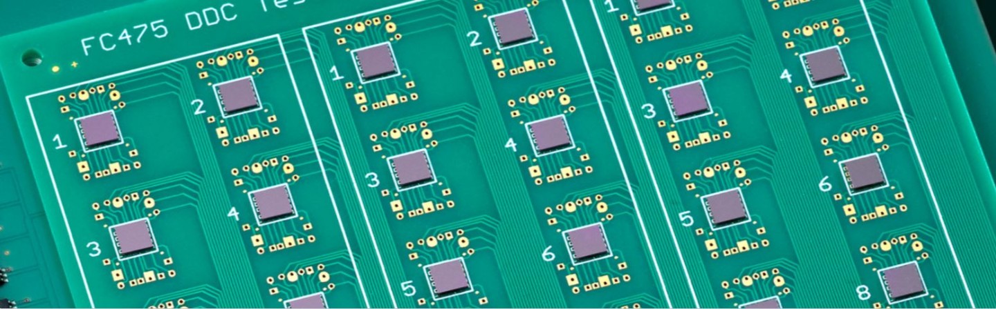
These test chips, which are already available, can be used to characterize soldered or bonded joints, for example. Appropriate contact resistance measurements during or after aging stresses can also be used to generate statements on the reliability of the connections produced. Another application are e.g. backside metallized test chips with a silver coating, which are available e.g. for sintering tests to optimize the sintering process for power semiconductors (use of different sintering pastes and processing parameters).
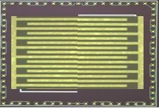
Test chips can also be used to measure surface resistances by means of comb structures on and under components.
In this way, it is possible to gain insights into the conditions under components under climatic load. Typical applications would be the evaluation of contamination, e.g. by solder flux, the determination of the quality of cleaning processes or the verification of the effectiveness of paint coatings.
Glass wafers, on the other hand, are often used for optical applications.
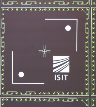
Nonius structures on glass chips are suitable for proving the positioning accuracy of machines during customer acceptance tests or at trade shows.
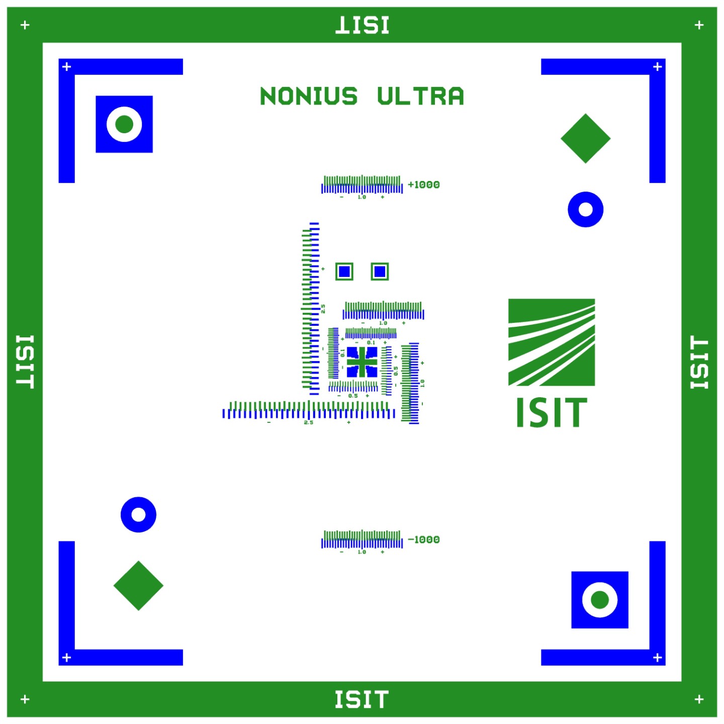
The optical structures are inserted into a substrate chip (blue) and a cover chip (green). With the help of the markings (aluminum pads) on the two chips, the placement accuracy (displacement, rotation) can be measured, e.g. by pick & place machines.
Test wafers offer versatile possibilities - only a few examples have been mentioned here. Please contact us if you are interested in already existing solutions. Surely you have your own ideas and wishes. We would be happy to work with you to develop new, challenging and interesting applications.
This might also interest you