Fraunhofer Institute for Silicon Technology
Dr. Michael Mensing
First AIScN-Based Ferroelectric Gate Field-Effect Transistors
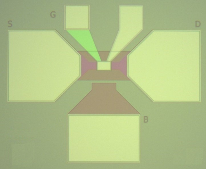
With the goal of creating technological conditions for increasing the efficiency of power transistors for power conversion, e-mobility and communication applications, the innovative material AlScN was successfully validated for its use in NMOS-transistors.
As such, the deliberate polarization switching of the ferroelectric AlScN in silicon-based transistors was demonstrated. This achievement represents an important proof of concept and underpins the potential of the novel approach by bridging the gap between materials research and first devices. For this purpose and based on process and device simulations, various transistor designs were tailored to the needs and strengths of the material system, whose ferroelectric properties were recently discovered by the MEMS applications business unit at the Fraunhofer ISIT.
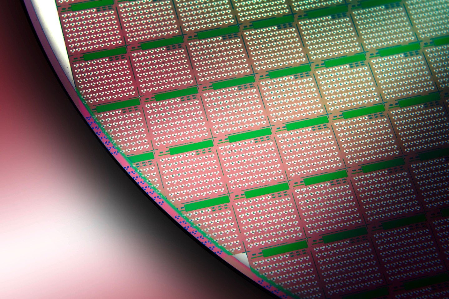
The designs were combined into a unified processing flow and fabricated in first iteration. The comprehensive electrical characterization of these unique devices is ongoing. However, based on the initial results the path to further improvements of the devices architecture has already been revealed. Besides the continuous integration in silicon-based transistors, a sophisticated roadmap has been laid out to tightly incorporate AlScN in the recently added GaN technology platform.
_________________________________
This discovery was made 2019 by the scientist Simon FIchtner at the Fraunhofer ISIT. Our researcher Simon Fichtner detected ferroelectricity for the first time in the III-V semiconductor-based material aluminum scandium nitride (AlScN).
Principle: As a piezoelectric material, AlScN generates electrical voltages when it is deformed and, conversely, the material changes shape when an electrical voltage is applied to it. This material can therefore be used to convert motion into electrical signals and electrical signals into motion. It is used for microdrives to drive chip speakers, for example, or to set tiny laser scanning mirrors in motion.