 Fraunhofer Institute for Silicon Technology
The semiconductor industry has been striving for decades to optimize the energy consumption, switching speed and area requirements of electronic components through miniaturization. The ever-increasing demand for highly efficient electronic components for many areas of data processing, network technology, communications, AI (artificial intelligence) and energy and machine management has made the semiconductor industry an indispensable technology for technical progress in the 20th and 21st centuries. Technical and economic investments in this field are correspondingly high.
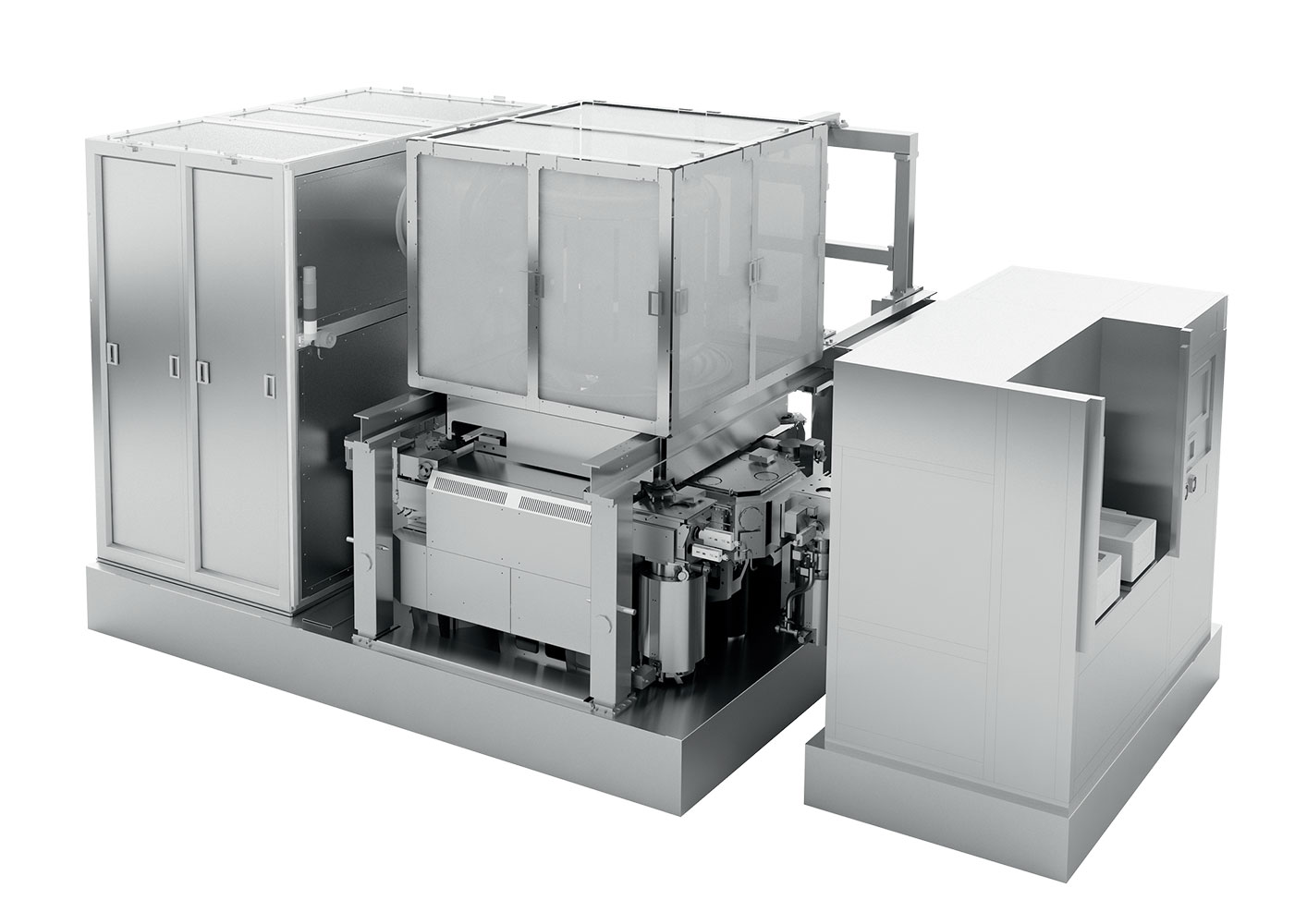
After more than 50 years of continuous miniaturization of structures, a number of current manufacturing technologies are reaching their limits. The world's only way out of this dilemma so far is offered by a novel technology: the electron multibeam mask writer, developed by Vienna-based IMS Nanofabrication GmbH. The key component for this device - an electron beam deflection chip - was developed by Fraunhofer ISIT.
Electron multi-beam mask writer for next generation chips
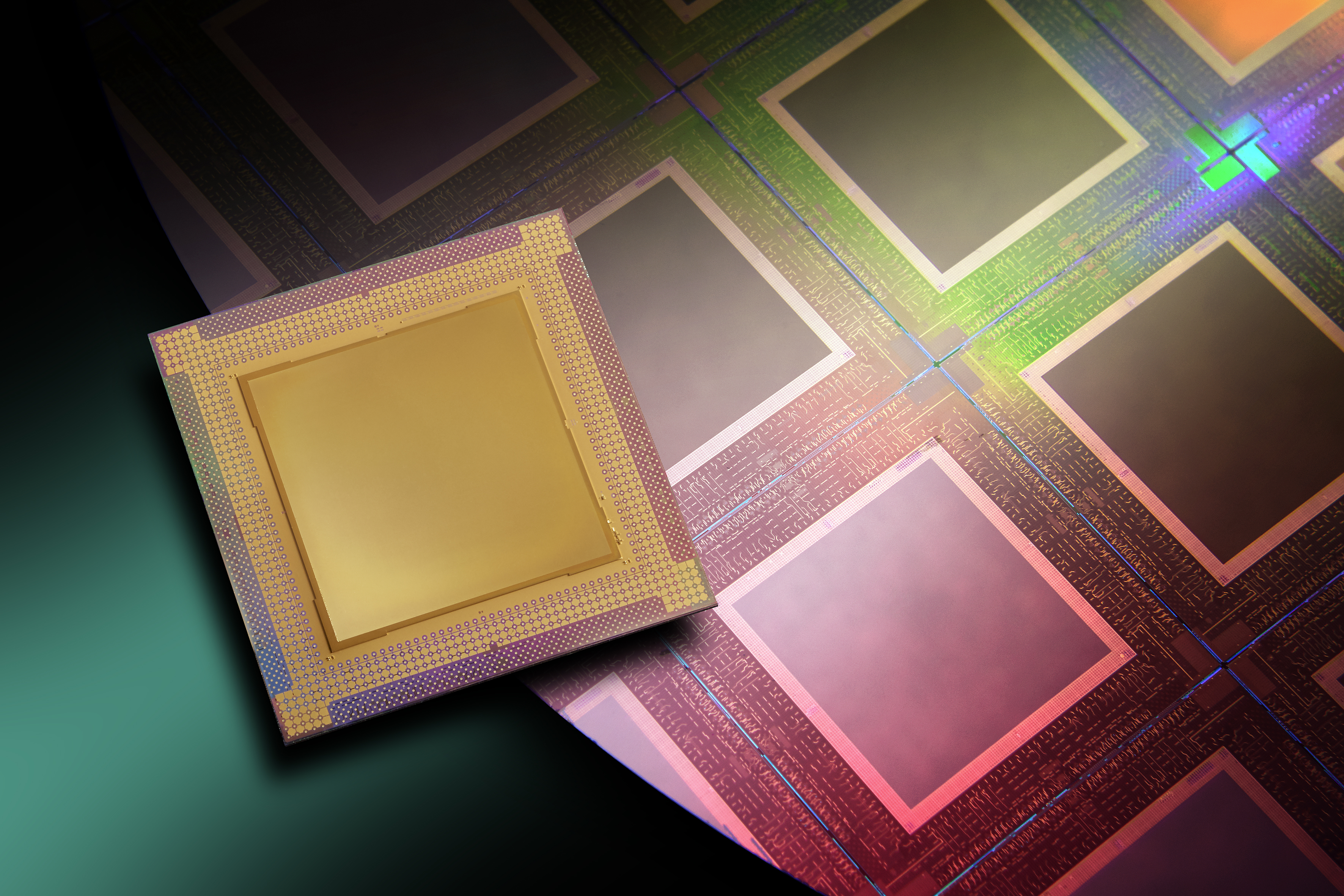
Chip structure
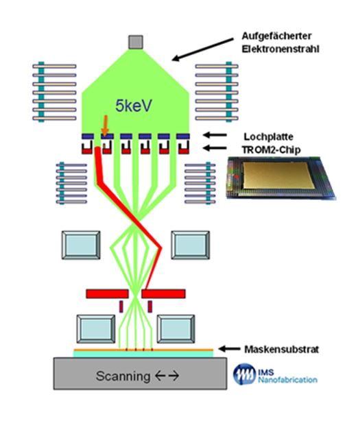
The basic principle of this chip is conceptually relatively simple: In the electron multi-beam mask writer a fanned-out electron beam is split into 512 x 512 = 262,144 individual beams by a perforated silicon plate. Each electron beam has a diameter of only a few micrometers. The 262,144 individual beams then hit the beam deflection chip, which is located downstream from the sensor. Its integrated a CMOS chip, together with the MEMS processing performed at ISIT, enables the targeted deflection of individual electron beams. This allows precise and selective exposure of the mask substrate located at the end of the beam path, from which photomasks are subsequently produced.
The MEMS components of the chip consist of apertures and gold electrodes through which the passing electrons can be deflected. To illustrate, the principle can be thought of as similar to that of an inkjet printer. The apertures are channels a few micrometers in size etched through the silicon CMOS chip. These channels, also called apertures, are each surrounded by high deflection and shielding electrodes made of galvanic gold. Each of these deflection electrodes is addressable via the integrated CMOS logic and can be energized. When voltage is applied, the passing electron beam is slightly deflected, rendering it ineffective. Deflected electron beams are filtered out by the downstream electron projection optics (shown in Figure 1a by rectangles and horizontal structures along the electron beam path). The CMOS logic allows the voltage state of each electrode to be switched on and off in the nanosecond range.
Challenges, goals & opportunities
All process challenges regarding defect freedom, shielding and preservation of CMOS logic could only be achieved by further development and refinement of existing MEMS procedures and technologies. Devices and media beyond the limits specified by manufacturers were used and evaluated. In many places, new procedural territory was broken and the limits of what was previously known were redefined. Over the course of the project, understanding of the intricate interaction of the more than 200 individual steps in the MEMS manufacturing chain of the deflection chip grew, increasing process reliability and consequently yield.
The new manufacturing process achieves imaging scales that could not be realized with any other technology to date. Therefore, there is no way around the electron multibeam mask recorder for further miniaturization in microelectronics.
ISIT scientists Martin Witt, Michael Kampmann and Dr. Jacqueline Atanelov from IMS Nanofabrication received the Fraunhofer Prize 2021 for their development work.
This might also interest you:
- Press release as PDF: Fraunhofer Prize 2021 for ISIT scientists Martin Witt, Michael Kampmann and Dr. Jacqueline Atanelov, IMS nanofabrication
- Video: Microchips for the production of semiconductors | Production, application, research
- Video: Microchips of the next generation! Making-Of about the winners of the Josef von Fraunhofer Prize 2021!