 Fraunhofer Institute for Silicon Technology
New paths for more powerful MEMS sensors
Crystallized thick a-Si:H layers
The aim of the study was to find out whether a-Si:H layers are suitable as a structural material for the surface micromechanics of MEMS inertial sensors. These sensors are usually based on silicon, as it is characterized by high electrical conductivity, mechanical stability and good thermal properties. In practice, approximately 80% of MEMS inertial sensors consist of thick poly-Si layers (10-18 μm) - with all the disadvantages of an energy-intensive manufacturing process.
For the study, p-type silicon (100) wafers with a diameter of 200 mm were used, which were coated with various SiO₂ types and then provided with a thick a-Si:H layer. The new method relies on a significantly lower deposition temperature and subsequent targeted crystallization. This not only makes the manufacturing process cheaper, but also more flexible and potentially more sustainable. In order to check the material quality, the a-Si:H layers were characterized in a variety of ways. The focus was on:
- Electrical conductivity: Higher crystallization temperatures promote the conversion from amorphous to crystalline silicon and improve conductivity. However, too much phosphorus doping has a counterproductive effect - it leads to defects and increased specific resistance.
- Mechanical stresses: These are strongly influenced by the process conditions. Two-stage annealing is particularly effective in reducing stresses in heavily doped layers.
- Crystallinity: X-ray diffraction measurements confirm the successful crystallization process. At the same time, it has been shown that excessive doping can interfere with crystal formation.
- Surface roughness: The a-Si:H layers have a significantly smoother surface than conventional epi-polycrystalline layers, especially at low PH₃ feed rates. This is an advantage for subsequent lithography.
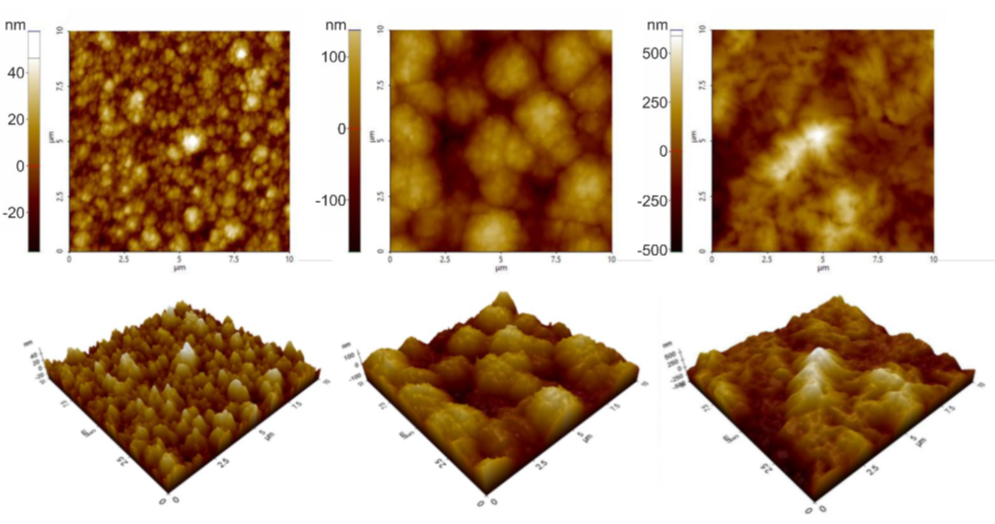
Figure 4 2D- and 3D AFM images of 750°C crystallized a-Si:H with various PH3 gas flow rate (left: 200 sccm, middle: 500 sccm) and epi-poly Si (right)
Why this approach is forward-looking
The major advantage of crystallized a-Si:H coatings lies in the energy-efficient, scalable manufacturing process. While conventional poly-Si coatings require expensive high-temperature processes, structuring is possible here at moderate temperatures. They are produced using thermal oxidation and plasma-enhanced chemical vapor deposition (PECVD) with silane (SiH₄) or tetraethylorthosilicate (TEOS).
At the same time, the new method offers many possibilities for targeted optimization: the control of doping, crystallization temperature and post-treatment specifically influences electrical, mechanical and structural properties. The study shows that thick, crystallized a-Si:H layers are an alternative to conventional poly-Si in MEMS production. They offer comparable - in some cases even better - properties at lower costs and energy consumption. However, further research is needed to exploit their full potential. In particular, the exact mechanisms of crystal formation and their dependence on the process parameters must be better understood. The future of MEMS could therefore not only be more powerful, but also more efficient.